A d v a n c e I n f o r m a t i o n
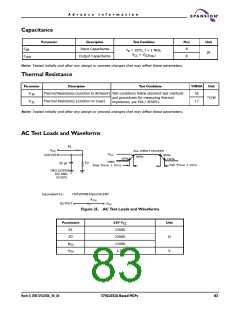
Capacitance
Parameter
Description
Te st Co nd i ti on
Max
8
Unit
CIN
Input Capacitance
Output Capacitance
TA = 25°C, f = 1 MHz,
VCC = VCC(typ.)
pF
COUT
8
Note: Tested initially and after any design or process changes that may affect these parameters.
Thermal Resistance
Parameter
Description
Test Conditions
VFBGA
Unit
θ JA
Thermal Resistance (Junction to Ambient) Test conditions follow standard test methods
and procedures for measuring thermal
55
°C/W
θ JC
Thermal Resistance (Junction to Case)
17
impedance, per EIA / JESD51.
Note: Tested initially and after any design or process changes that may affect these parameters.
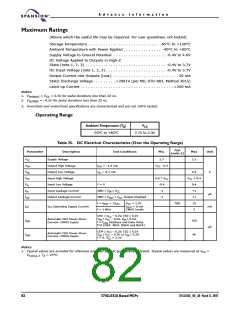
AC Test Loads and Waveforms
R1
VCC
ALL INPUT PULSES
90%
10%
Fall Time: 1 V/ns
V
CC
OUTPUT
90%
10%
GND
Rise Time: 1 V/ns
R2
30 pF
INCLUDING
JIG AND
SCOPE
Equivalent to:
THÉVENINEQUIVALENT
RTH
OUTPUT
VTH
Figure 25. AC Test Loads and Waveforms
Parameters
3.0V VCC
22000
22000
11000
1.50
Unit
R1
R2
Ω
RTH
VTH
V
March 31, 2005 S71GL032A_00_A0
S71GL032A Based MCPs
83

 SPANSION [ SPANSION ]