A d v a n c e I n f o r m a t i o n
Configuration Register
The device contains a Configuration Register for configuring read accesses. The
Configuration Register is accessed by the Configuration Register Read and the
Configuration Register Write commands. The Configuration Register does not oc-
cupy any addressable memory location, but rather, is accessed by the
Configuration Register commands. The Configuration Register is readable any
time, however, writing the Configuration Register is restricted to times when the
Embedded Algorithm™ is not active. If the user attempts to write the Configura-
tion Register while the Embedded Algorithm™ is active, the write operation is
ignored and the contents of the Configuration Register remain unchanged.
The Configuration Register is a 16 bit data field which is accessed by DQ15–DQ0.
During a read operation, DQ31–DQ16 returns all zeroes. Table 9 shows the Con-
figuration Register. Also, Configuration Register reads operate the same as
Autoselect command reads. When the command is issued, the bank address is
latched along with the command. Reads operations to the bank that was specified
during the Configuration Register read command return Configuration Register
contents. Read operations to the other bank return flash memory data. Either
bank address is permitted when writing the Configuration Register read
command.
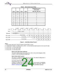
Table 9. Configuration Register Definitions
CR15
CR14
CR13
CR12
CR11
CR10
CR9
CR8
RM
Reserved
IAD3
IAD2
IAD1
IAD0
DOC
WC
CR7
CR6
CR5
CR4
CR3
CR2
CR1
CR0
BS
CC
Reserved
Reserved
Reserved
BL2
BL1
BL0
Configuration Register
CR15 = Read Mode (RM)
0 = Synchronous Burst Reads Enabled
1 = Asynchronous Reads Enabled (Default)
CR14 = Reserved for Future Enhancements
These bits are reserved for future use. Set these bits to “0”.
March 22, 2004 30606B0
S29CD032G
25

 SPANSION [ SPANSION ]