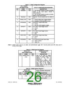
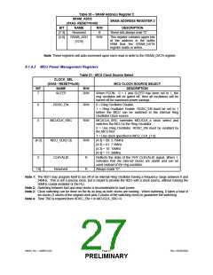
Table 20 – SRAM Address Register 2
SRAM_ADD2
(0XA2- RESET=0x00)
SRAM ADDRESS REGISTER 2
BIT
[7:3]
[2:0]
NAME
Reserved
SRAM_ADD
[10:8]
R/W
DESCRIPTION
R
These bits always read “0”.
R/W
This register contains upper bits
of the address in the buffer
RAM that the SRAM_DATA
register reads or writes.
Note: These registers will auto increment upon each read or write to the SRAM_DATA register.
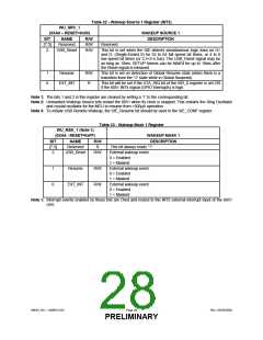
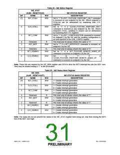
6.1.4.3 MCU Power Management Registers
Table 21 - MCU Clock Source Select
CLOCK_SEL
(0XA5 - RESET=0x40)
NAME
MCU CLOCK SOURCE SELECT
BIT
R/W
DESCRIPTION
7
SLEEP
R/W
When PCON. 0 = 1 and SLEEP has been set to 1, the
ring oscillator will be gated off, then all oscillators will be
turned off for maximum power savings.
6
5
ROSC_EN
R/W
R/W
0 = Ring Oscillator Disable.
1 = Ring Oscillator Enable. ROSC_EN must be set to 1
before the MCU can be switched to the internal Ring
Oscillator Clock source.
MCUCLK_SRC
MCUCLK_SRC overrides MCUCLK_x clock select and
switches the MCU to the Ring Oscillator.
0 = Use Ring Oscillator. ROSC_EN must be enabled by
the MCU first.
1 = Use clock specified in MCU_CLK_[1:0]
[4:3] = 00: 3.75MHz
[4:3]
MCU_CLK[1:0]
R/W
[4:3] = 01: 7.5MHz
[4:3] = 10: 15MHz
[4:3] = 11: 30MHz
2
CLKVALID
Reserved
R
R
Reflects the state of the PHY CLKVALID signal. When 1,
indicates that the internal clocks are stable and can be
used instead of the ring oscillator.
1:0]
Always reads “0”.
Note 1: The 8051 may program itself to run off of an internal Ring Oscillator having a frequency range between 8 and
24MHz. This is not a precise clock, but is meant to provide the 8051 with a clock source, without running the
30MHz crystal oscillator or the PLL
Note 2: Switching between fast and slow clocks is recommended to save power.
Note 3: Clock switching can be done on the fly as long as both clocks are running. When switching, it takes a total of
six clocks (3 clocks of the original clock plus 3 clocks of the switching clock) to guarantee the switching.
Note 4: Time TBD is required from ROSC_EN=1 to MCUCLK_SRC=0.
SMSC DS – USB97C201
Page 27
Rev. 03/25/2002
PRELIMINARY

 SMSC [ SMSC CORPORATION ]