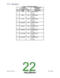
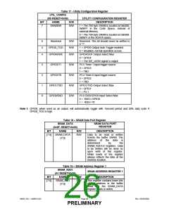
Table 17 - Utility Configuration Register
UTIL_CONFIG
(9D RESET=0x00)
NAME
UTILITY CONFIGURATION REGISTER
DESCRIPTION
BIT
R/W
7
SRAMSW
R/W
1 = The 768 byte SRAM is located at 0x0400-
0x06FF in the Code Space, instead of
external Memory.
0 = The 768 byte SRAM is located at 0x0400-
0x06FF in the XDATA space.
6
5
Reserved
R/W
R/W
Reserved. This bit should never be written to
a “1”.
GPIO0_TOG
1 = GPIO0 Output Auto Toggle enabled.
0 = Disabled, normal operation occurs.
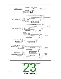
GPIO4/SOF Output Select Mux
0 = GPIO4
1 = The IDE_nIOW signal is output.
P3.5 Timer 1 input trigger source
0 = GPIO3
4
3
2
1
0
GPIO4/nWE
GPIO3/T1
R/W
R/W
R/W
R/W
R/W
1 = TBD
GPIO2/T0
P3.4 Timer 0 input trigger source
0 = GPIO2
1 = TBD
GPIO1/TXD
GPIO0/RXD
GPIO1/TXD Output Select Mux
0 = GPIO1
1 = P3.1
P3.0 RXD/GPIO0 Input Select Mux
0 = RXD<=GPIO0
1 = RXD<='0'
Note 1: GPIO0, when used as an output, will automatically toggle with 1second period and 50% duty cycle if
GPIO0_TOG is high.
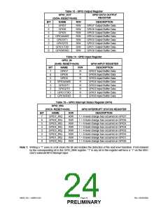
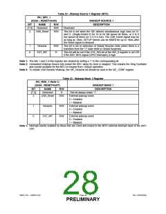
Table 18 – SRAM Data Port Register
SRAM_DATA
SRAM DATA PORT
REGISTER
(0x9F- RESET=0x00)
BIT
NAME
R/W
R/W
DESCRIPTION
[7:0] SRAM_DATA
[7:0]
Data to be read or written
from/to the buffer SRAM. The
address of the data is
determined
by
the
SRAM_ADD1/2 registers. Data
to be written will be done so
upon write of this register.
While reads of the register
always reflects the data at the
memory location.
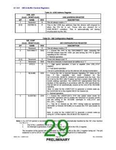
Table 19 – SRAM Address Register 1
SRAM_ADD1
SRAM ADDRESS REGISTER 1
(A1 RESET=0x00)
BIT
NAME
SRAM_ADD
[7:0]
R/W
DESCRIPTION
[7:0]
R/W
This register contains lower bits
of the address in the buffer
RAM that the SRAM_DATA
register reads or writes.
SMSC DS – USB97C201
Page 26
Rev. 03/25/2002
PRELIMINARY

 SMSC [ SMSC CORPORATION ]