Highly Integrated Full Featured Hi-Speed USB 2.0 ULPI Transceiver
Datasheet
the Link can disable the pull-up resistor on STP. When RESETB is low the Interface Protect Circuit
will be disabled.
6.4
Full Speed/Low Speed Serial Modes
The USB3320 includes two serial modes to support legacy Links which use either the 3pin or 6pin
serial format. To enter either serial mode, the Link will need to write a 1 to the 6-pin FsLsSerialMode
or the 3-pin FsLsSerialMode bits in the Interface control register. Serial Mode may be used to conserve
power when attached to a device that is not capable of operating in Hi-Speed.
The serial modes are entered in the same manner as the entry into Low Power Mode. The Link writes
the Interface Control register bit for the specific serial mode. The USB3320 will assert DIR and shut
off the clock after at least five clock cycles. Then the data bus goes to the format of the serial mode
selected. Before entering Serial Mode the Link must set the ULPI transceiver to the appropriate mode
as defined in Table 5.1.
In ULPI Output Clock Mode, the transceiver will shut off the 60MHz clock to conserve power. Should
the Link need the 60MHz clock to continue during the serial mode of operation, the ClockSuspendM
bit[3] of the Interface Control Register should be set before entering a serial mode. If set, the 60 MHz
clock will be present during serial modes.
In serial mode, interrupts are possible from unmasked sources. The state of each interrupt source is
sampled prior to the assertion of DIR and this is compared against the asynchronous level from
interrupt source.
Exiting the serial modes is the same as exiting Low Power Mode. The Link must assert STP to signal
the transceiver to exit serial mode. When the transceiver can accept a command, DIR is de-asserted
and the transceiver will wait until the Link de-asserts STP to resume synchronous ULPI operation. The
RESETB pin can also be pulsed low to reset the USB3320 and return it to Synchronous Mode.
6.4.0.1
3pin FS/LS Serial Mode
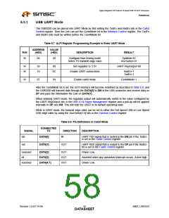
Three pin serial mode utilizes the data bus pins for the serial functions shown in Table 6.5.
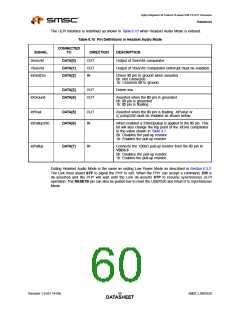
Table 6.5 Pin Definitions in 3 Pin Serial Mode
CONNECTED
SIGNAL
TO
DIRECTION
DESCRIPTION
tx_enable
data
DATA[0]
DATA[1]
IN
Active High transmit enable.
I/O
TX differential data on DP/DM when tx_enable is high.
RX differential data from DP/DM when tx_enable is low.
SE0
DATA[2]
I/O
TX SE0 on DP/DM when tx_enable is high.
RX SE0_b from DP/DM when tx_enable is low.
interrupt
DATA[3]
OUT
OUT
Asserted when any unmasked interrupt occurs. Active high.
Driven Low.
Reserved
DATA[7:4]
Revision 1.0 (07-14-09)
SMSC USB3320
DATA5S6HEET

 SMSC [ SMSC CORPORATION ]