Highly Integrated Full Featured Hi-Speed USB 2.0 ULPI Transceiver
Datasheet
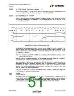
CLK
DATA[7:0]
DIR
Turn
around
Rxd
Cmd
Rxd
Cmd
Turn
around
Idle
PID
D1
D2
STP
NXT
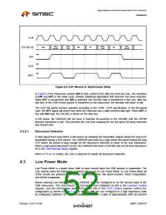
Figure 6.8 ULPI Receive in Synchronous Mode
In Figure 6.8 the transceiver asserts DIR to take control of the data bus from the Link. The assertion
of DIR and NXT in the same cycle contains additional information that Rxactive has been asserted.
When NXT is de-asserted and DIR is asserted, the RXCMD data is transferred to the Link. After the
last byte of the USB receive packet is transferred to the transceiver, the linestate will return to idle.
The ULPI full speed receiver operates according to the UTMI / ULPI specification. In the full speed
case, the NXT signal will assert only when the Data bus has a valid received data byte. When NXT is
low with DIR high, the RXCMD is driven on the data bus.
In full speed, the USB3320 will not issue a Rxactive de-assertion in the RXCMD until the DP/DM
linestate transitions to idle. This prevents the Link from violating the two full speed bit times minimum
turn around time.
6.2.5.1
Disconnect Detection
A High Speed host must detect a disconnect by sampling the transmitter outputs during the long EOP
transmitted during a SOF packet. The USB3320 only looks for a high speed disconnect during the long
EOP where the period is long enough for the disconnect reflection to return to the host transceiver.
When a high speed disconnect occurs, the USB3320 will return a RXCMD and set the host disconnect
bit in the USB Interrupt Status register.
When in FS or LS modes, the Link is expected to handle all disconnect detection.
6.3
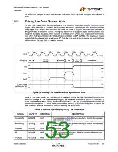
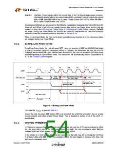
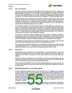
Low Power Mode
Low Power Mode is a power down state to save current when the USB session is suspended. The
Link controls when the transceiver is placed into or out of Low Power Mode. In Low Power Mode all
of the circuits are powered down except the interface pins, full speed receiver, VBUS comparators,
and IdGnd comparator.
Before entering Low Power Mode, the USB3320 must be configured to set the desired state of the
USB transceiver. The XcvrSelect[1:0], TermSelect and OpMode[1:0] bits in the Function Control
register, and the DpPulldown and DmPulldown bits in the OTG Control register control the
configuration as shown in Table 5.1. The DP and DM pins are configured to a high impedance state
by configuring OpMode[1:0] = 01. Pull-down resistors with a value of approximately 2MΩ are present
Revision 1.0 (07-14-09)
SMSC USB3320
DATA5S2HEET

 SMSC [ SMSC CORPORATION ]