Highly Integrated Full Featured Hi-Speed USB 2.0 ULPI Transceiver
Datasheet
register data. At T4, the transceiver will accept the register data and drive NXT low. The Link will drive
an Idle on the bus and drive STP high to signal the end of the data packet. Finally, at T5, the
transceiver will latch the data into the register and the Link will pull STP low.
NXT is used to control when the Link drives the register data on the bus. DIR is low throughout this
transaction since the transceiver is receiving data from the Link. STP is used to end the transaction
and data is registered after the de-assertion of STP. After the write operation completes, the Link must
drive a ULPI Idle (00h) on the data bus or the USB3320 may decode the bus value as a ULPI
command.
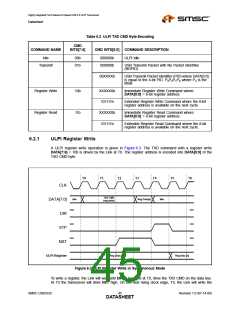
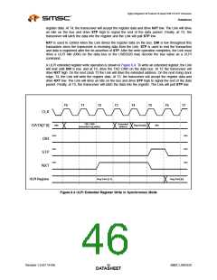
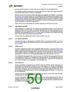
A ULPI extended register write operation is shown in Figure 6.4. To write an extended register, the Link
will wait until DIR is low, and at T0, drive the TXD CMD on the data bus. At T2 the transceiver will
drive NXT high. On the next clock T3 the Link will drive the extended address. On the next rising clock
edge, T4, the Link will write the register data. At T5, the transceiver will accept the register data and
drive NXT low. The Link will drive an Idle on the bus and drive STP high to signal the end of the data
packet. Finally, at T5, the transceiver will latch the data into the register. The Link will pull STP low.
T0
T1
T2
T3
T4
T5
T6
T7
CLK
DATA[7:0]
DIR
TXD CMD
(extended reg write)
Extended
address
Idle
Reg Data[n]
Idle
STP
NXT
Reg Data [n-1]
Reg Data [n]
ULPI Register
Figure 6.4 ULPI Extended Register Write in Synchronous Mode
Revision 1.0 (07-14-09)
SMSC USB3320
DATA4S6HEET

 SMSC [ SMSC CORPORATION ]