Highly Integrated Full Featured Hi-Speed USB 2.0 ULPI Transceiver
Datasheet
Chapter 6 ULPI Operation
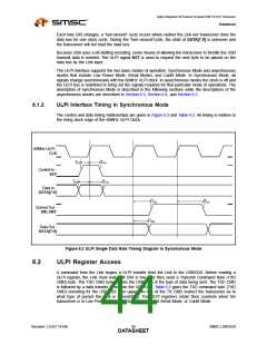
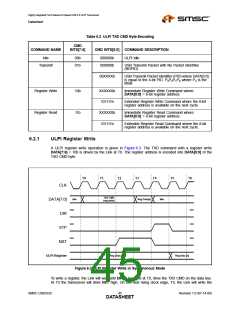
6.1
Overview
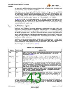
The USB3320 uses the industry standard ULPI digital interface to facilitate communication between
the USB Transceiver (PHY) and Link (device controller). The ULPI interface is designed to reduce the
number of pins required to connect a discrete USB Transceiver to an ASIC or digital controller. For
example, a full UTMI+ Level 3 OTG interface requires 54 signals while a ULPI interface requires only
12 signals.
The ULPI interface is documented completely in the “UTMI+ Low Pin Interface (ULPI) Specification
Revision 1.1”. The following sections describe the operating modes of the USB3320 digital interface.
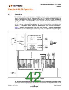
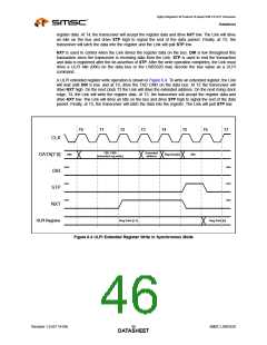
Figure 6.1 illustrates the block diagram of the ULPI digital functions. It should be noted that this
USB3320 does not use a “ULPI wrapper” around a UTMI+ PHY core as the ULPI specification implies.
USB Transmit and Receive Logic
Tx Data
HSTx Data
High Speed TX
Data[7:0]
To TX
Analog
Full Speed TX
Low Speed TX
FS/LS Tx Data
DIR
NOTE:
ULPI Protocol
Block
The ULPI interface
is a wrapperless
design.
NXT
STP
Rx Data
High Speed Data
Recovery
Full / Low Speed
Data Recovery
HS RX Data
FS/LS Data
To RX
Analog
To
OTG
To USB
Audio
Analog
Analog
Rid State
Machine
Interrupt Control
RESETB
POR
ULPI Register Array
Figure 6.1 ULPI Digital Block Diagram
The advantage of a “wrapper less” architecture is that the USB3320 has a lower USB latency than a
design which must first register signals into the PHY’s wrapper before the transfer to the PHY core. A
Revision 1.0 (07-14-09)
SMSC USB3320
DATA4S2HEET

 SMSC [ SMSC CORPORATION ]