Highly Integrated Full Featured Hi-Speed USB 2.0 ULPI Transceiver
Datasheet
low latency PHY allows a Link to use a wrapper around a UTMI Link and still make the required USB
turn-around timing given in the USB 2.0 specification.
RxEndDelay maximum allowed by the UTMI+/ULPI for 8-bit data is 63 high speed clocks. USB3320
uses a low latency high speed receiver path to lower the RxEndDelay to 43 high speed clocks. This
low latency design gives the Link more cycles to make decisions and reduces the Link complexity. This
is the result of the “wrapper less” architecture of the USB3320. This low RxEndDelay should allow
legacy UTMI Links to use a “wrapper” to convert the UTMI+ interface to a ULPI interface.
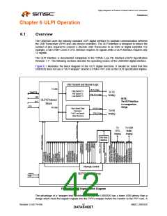
In Figure 6.1, a single ULPI Protocol Block decodes the ULPI 8-bit bi-directional bus when the Link
addresses the PHY. The Link must use the DIR output to determine direction of the ULPI data bus.
The USB3320 is the “bus arbitrator”. The ULPI Protocol Block will route data/commands to the
transmitter or the ULPI register array.
6.1.1
ULPI Interface Signals
The UTIM+ Low Pin Interface (ULPI) uses twelve pins to connect a full OTG Host / Device USB
Transceiver to an SOC. A reduction of external pins on the transceiver is accomplished by realizing
that many of the relatively static configuration pins (xcvrselect[1:0], termselect, opmode[1:0], and
DpPullDown DmPulldown to list a few,) can be implemented by having an internal static register array.
An 8-bit bi-directional data bus clocked at 60MHz allows the Link to access this internal register array
and transfer USB packets to and from the transceiver. The remaining 3 pins function to control the
data flow and arbitrate the data bus.
Direction of the 8-bit data bus is controlled by the DIR output from the transceiver. Another output,
NXT, is used to control data flow into and out of the device. Finally, STP, which is in input to the
transceiver, terminates transfers and is used to start up and resume from Low Power Mode.
The twelve signals are described below in Table 6.1.
Table 6.1 ULPI Interface Signals
SIGNAL
DIRECTION
DESCRIPTION
CLK
I/O
60MHz ULPI clock. All ULPI signals are driven synchronous to the rising edge of
this clock. This clock can be either driven by the transceiver or the Link as
described in Section 5.4.1
DATA[7:0]
I/O
8-bit bi-directional data bus. Bus ownership is determined by DIR. The Link and
transceiver initiate data transfers by driving a non-zero pattern onto the data bus.
ULPI defines interface timing for a single-edge data transfers with respect to rising
edge of the ULPI clock.
DIR
OUT
Controls the direction of the data bus. When the transceiver has data to transfer
to the Link, it drives DIR high to take ownership of the bus. When the transceiver
has no data to transfer it drives DIR low and monitors the bus for commands from
the Link. The transceiver will pull DIR high whenever the interface cannot accept
data from the Link, such as during PLL start-up.
STP
NXT
IN
The Link asserts STP for one clock cycle to stop the data stream currently on the
bus. If the Link is sending data to the transceiver, STP indicates the last byte of
data was on the bus in the previous cycle.
OUT
The transceiver asserts NXT to throttle the data. When the Link is sending data to
the transceiver, NXT indicates when the current byte has been accepted by the
transceiver. The Link places the next byte on the data bus in the following clock
cycle.
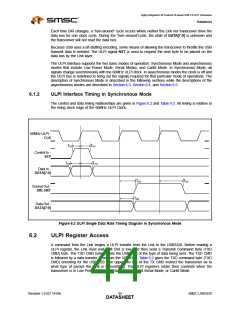
USB3320 implements a Single Data Rate (SDR) ULPI interface with all data transfers happening on
the rising edge of the 60MHz ULPI Clock while operating in Synchronous Mode. The direction of the
data bus is determined by the state of DIR. When DIR is high, the transceiver is driving DATA[7:0].
When DIR is low, the Link is driving DATA[7:0].
SMSC USB3320
Revision 1.0 (07-14-09)
DATA4S3HEET

 SMSC [ SMSC CORPORATION ]