Highly Integrated Full Featured Hi-Speed USB 2.0 ULPI Transceiver
Datasheet
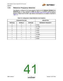
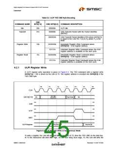
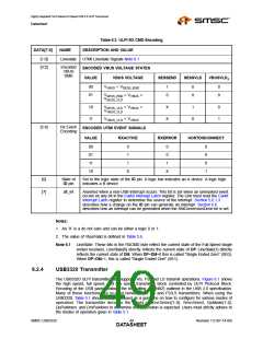
Table 6.2 ULPI TXD CMD Byte Encoding
CMD
BITS[7:6]
COMMAND NAME
CMD BITS[5:0] COMMAND DESCRIPTION
Idle
00b
01b
000000b
000000b
ULPI Idle
Transmit
USB Transmit Packet with No Packet Identifier
(NOPID)
00XXXXb
USB Transmit Packet Identifier (PID) where DATA[3:0]
is equal to the 4-bit PID. P3P2P1P0 where P3 is the
MSB.
Register Write
Register Read
10b
11b
XXXXXXb
101111b
Immediate Register Write Command where:
DATA[5:0] = 6-bit register address
Extended Register Write Command where the 8-bit
register address is available on the next cycle.
XXXXXXb
101111b
Immediate Register Read Command where:
DATA[5:0] = 6-bit register address
Extended Register Read Command where the 8-bit
register address is available on the next cycle.
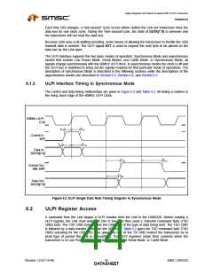
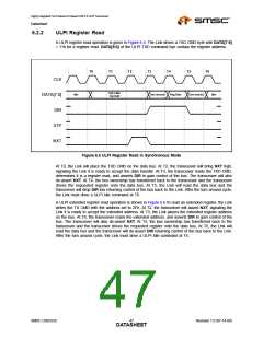
6.2.1
ULPI Register Write
A ULPI register write operation is given in Figure 6.3. The TXD command with a register write
DATA[7:6] = 10b is driven by the Link at T0. The register address is encoded into DATA[5:0] of the
TXD CMD byte.
T0
T1
T2
T3
T4
T5
T6
CLK
DATA[7:0]
DIR
TXD CMD
(reg write)
Idle
Reg Data[n]
Idle
STP
NXT
Reg Data [n-1]
Reg Data [n]
ULPI Register
Figure 6.3 ULPI Register Write in Synchronous Mode
To write a register, the Link will wait until DIR is low, and at T0, drive the TXD CMD on the data bus.
At T2 the transceiver will drive NXT high. On the next rising clock edge, T3, the Link will write the
SMSC USB3320
Revision 1.0 (07-14-09)
DATA4S5HEET

 SMSC [ SMSC CORPORATION ]