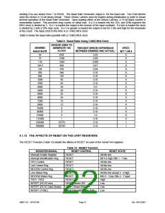
dividing it by any divisor from 1 to 65535. The Baud Rate Generator output is 16x the baud rate. Two 8-bit latches
store the divisor in 16-bit binary format. These Divisor Latches must be loaded during initialization in order to insure
desired operation of the Baud Rate Generator. Upon loading either of the Divisor Latches, a 16 bit Baud counter is
immediately loaded. This prevents long counts on initial load. If a 0 is loaded into the DDL and DDM registers the
BRG clock is divided by 3. If a 1 is loaded the output is the inverse of the input oscillator. If a two is loaded the clock
is divided by 2 with a 50% duty cycle. If a 3 or greater is loaded the output is low for 2 bits and high for the remainder
of the count. The input clock to the BRG is a 1.8462 MHz clock.
Table 9 shows the baud rates possible with a 1.8462 MHz clock.
Table 9 - Baud Rates Using 1.8462 MHz Clock
DIVISOR USED TO
DESIRED
BAUD RATE
50
GENERATE 16X
CLOCK
CROC:
PERCENT ERROR DIFFERENCE
BETWEEN DESIRED AND ACTUAL*
BIT 7 OR 6
2307
1538
1049
858
769
384
192
96
0.03
0.03
0.005
0.01
0.03
0.16
0.16
0.16
0.16
0.5
X
X
X
X
X
X
X
X
X
X
X
X
X
X
X
X
X
X
X
1
75
110
134.5
150
300
600
1200
1800
2000
2400
3600
4800
7200
64
58
48
32
24
16
12
6
3
2
0.16
0.16
0.16
0.16
0.16
0.16
0.16
1.6
9600
19200
38400
57600
115200
230400
460800
1
0.16
0.16
0.16
32770
32769
1
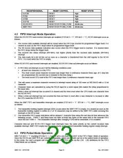
4.1.12 THE AFFECTS OF RESET ON THE UART REGISTERS
The RESET Function (Table 10) details the affects of RESET on each of the Serial Port registers.
Table 10 - RESET Function
REGISTER/SIGNAL
Interrupt Enable Register
Interrupt Identification Reg.
FIFO Control
RESET CONTROL
RESET STATE
All bits low
Bit 0 is high; Bits 1 - 7 low
RESET
RESET
RESET
All bits low
Line Control Reg.
RESET
All bits low
MODEM Control Reg.
Line Status Reg.
RESET
RESET
All bits low
All bits low except 5 - 6 high
MODEM Status Reg.
TXD1, TXD2
INTRPT (RCVR errs)
INTRPT (RCVR Data Ready)
INTRPT (THRE)
RESET
RESET
RESET/Read LSR
RESET/Read RBR
RESET/ReadIIR/Write THR
Bits 0 - 3 low; Bits 4 - 7 input
High
Low
Low
Low
SMSC DS – SP37E760
Page 22
Rev. 04/13/2001

 SMSC [ SMSC CORPORATION ]