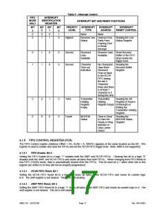
4.1.8.7
Transmitter Empty, Bit 6
The Transmitter Empty (TEMT) bit is set to a logic “1” whenever the Transmitter Holding Register (THR) and
Transmitter Shift Register (TSR) are both empty. It is reset to logic “0” whenever either the THR or TSR contains a
data character. Bit 6 is read-only. In the FIFO mode this bit is set whenever the THR and TSR are both empty.
4.1.8.8
RCVR FIFO Error, Bit 7
The RCVR FIFO Error bit is permanently set to logic “0” in the 450 mode. In the FIFO mode this bit is set to a logic
“1” when there is at least one parity error, framing error or break indication in the FIFO. This bit is cleared when the
LSR is read if there are no subsequent errors in the FIFO.
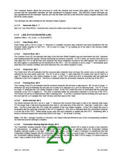
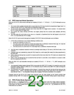
4.1.9 MODEM STATUS REGISTER (MSR)
The Modem Status register (Address Offset = 6H, DLAB = X, READ/WRITE) provides the current state of the control
lines from the MODEM or peripheral device. In addition to this current state information, four bits of the MODEM
Status Register provide state change information. These four bits are set to logic “1” whenever a control input
from the MODEM changes state. They are reset to logic “0” whenever the MODEM Status Register is read.
4.1.9.1
Delta Clear To Send, Bit 0
The Delta Clear To Send (DCTS) bit indicates that the nCTS input to the chip has changed state since the last
time the MSR was read.
4.1.9.2
Delta Data Set Ready, Bit 1
The Delta Data Set Ready (DDSR) bit indicates that the nDSR input has changed state since the last time the MSR
was read.
4.1.9.3
Trailing Edge Of Ring Indicator, Bit 2
The Trailing Edge of Ring Indicator (TERI) bit indicates that the nRI input has changed from logic “0” to logic “1”.
4.1.9.4
Delta Data Carrier Detect, Bit 3
The Delta Data Carrier Detect (DDCD) bit indicates that the nDCD input to the chip has changed state.
Note: Whenever bits 0, 1, 2, or 3 are set to a logic “1”, a MODEM Status Interrupt is generated.
4.1.9.5
Clear To Send, Bit 4
The Clear To Send bit is the complement of the Clear To Send input (nCTS). If the Loop bit of the MCR is set to logic
“1”, this bit is equivalent to nRTS in the MCR.
4.1.9.6
Data Set Ready, Bit 5
The Data Set Ready bit is the complement of the Data Set Ready input (nDSR). If the Loop bit of the MCR is set to
logic “1”, this bit is equivalent to DTR in the MCR.
4.1.9.7
Ring Indicator, Bit 6
The Ring Indicator bit is the complement of the Ring Indicator input (nRI). If the Loop bit of the MCR is set to logic
“1”, this bit is equivalent to OUT1 in the MCR.
4.1.9.8
Data Carrier Detect, Bit 7
The Data Carrier Detect bit is the complement of the Data Carrier Detect input (nDCD). If the Loop bit of the MCR is
set to logic “1”, this bit is equivalent to OUT2 in the MCR.
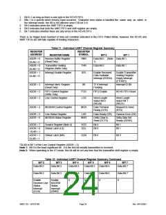
4.1.10 SCRATCHPAD REGISTER (SCR)
The Scratchpad register (Address Offset =7H, DLAB =X, READ/WRITE) has no effect on the operation of the Serial
Port. It is intended as a scratchpad register to be used by the programmer to hold data temporarily.
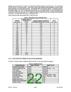
4.1.11 PROGRAMMABLE BAUD RATE GENERATOR DIVISOR LATCHES
The internal Baud Rate Generator (BRG) using the Programmable Baud Rate Generator Divisor Latches DDL and
DDM (Address Offset = 0 and 1, DLAB = 1, READ/WRITE) is capable of taking any clock input (DC to 3 MHz) and
SMSC DS – SP37E760
Page 21
Rev. 04/13/2001

 SMSC [ SMSC CORPORATION ]