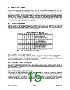
4.1.6.3
Parity Enable, Bit 3
When the Parity Enable bit is a logic “1” a parity bit is generated (transmit data) or checked (receive data) between
the last data word bit and the first stop bit of the serial data. The parity bit is used to generate an even or odd number
of 1s when the data word bits and the parity bit are summed.
4.1.6.4
Even Parity Select, Bit 4
When the Even Parity Select (EPS) bit is a logic “0” and the Parity Enable is a logic “1”, an odd number of logic “1”’s
is transmitted or checked in the data word and the parity bit. When the Parity Enable is a logic “1” and the EPS bit is
a logic “1” an even number of bits is transmitted and checked.
4.1.6.5
Stick Parity, Bit 5
When the Stick Parity bit is a logic “1” and the Parity Enable is a logic “1”, the parity bit is transmitted and then
detected by the receiver in the opposite state indicated by the EPS bit.
4.1.6.6
Set Break, Bit 6
When the Set Break Control bit is a logic “1”, the transmit data output (TXD) is forced to the Spacing or logic “0” state
and remains there until reset by a low level bit 6, regardless of other transmitter activity. This feature enables the
Serial Port to alert a terminal in a communications system.
4.1.6.7
DLAB, Bit 7
The Divisor Latch Access Bit must be set high (logic “1”) to access the Divisor Latches of the Baud Rate Generator
during read or write operations. It must be set low (logic “0”) to access the Receiver Buffer Register, the Transmitter
Holding Register, or the Interrupt Enable Register.
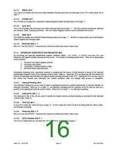
4.1.7 MODEM CONTROL REGISTER (MCR)
The Modem Control register (Address Offset = 4H, DLAB = X, READ/WRITE) manages the interface for the MODEM,
data set, or device emulating a MODEM.
4.1.7.1
Data Terminal Ready, Bit 0
The Data Terminal Ready bit controls the Data Terminal Ready (nDTR) output. When bit 0 is set to a logic “1”,
the nDTR output is forced to a logic “0”. When bit 0 is a logic “0”, the nDTR output is forced to a logic “1”.
Request To Send, Bit 1
The Request To Send bit controls the Request To Send (nRTS) output. . When bit 1 is set to a logic “1”, the
nRTS output is forced to a logic “0”. When bit 1 is a logic “0”, the nRTS output is forced to a logic “1”.
4.1.7.2
OUT1, Bit 2
The OUT1 bit controls the Output 1 (OUT1) bit. This bit does not have an output pin and can only be read or written
by the CPU.
4.1.7.3
OUT2, Bit 3
The OUT2 bit is used to enable the UART interrupt. When OUT2 is a logic “0”, the serial port interrupt output is
forced to a high impedance state; i.e, disabled. When OUT2 is a logic “1”, the serial port interrupt outputs are
enabled.
4.1.7.4
Loop, Bit 4
The Loop bit provides the loopback feature for diagnostic testing of the Serial Port. When bit 4 is set to logic “1”, the
following occurs:
1. The TXD is set to the Marking State (logic “1”).
2. The receiver Serial Input (RXD) is disconnected.
3. The output of the Transmitter Shift Register is “looped back” into the Receiver Shift Register input.
4. All MODEM Control inputs (nCTS, nDSR, nRI and nDCD) are disconnected.
5. The four MODEM Control outputs (nDTR, nRTS, OUT1 and OUT2) are internally connected to the four
MODEM Control inputs (nDSR, nCTS, RI and DCD) respectively.
6. The Modem Control output pins are forced inactive.
7. Data that is transmitted is immediately received.
SMSC DS – SP37E760
Page 19
Rev. 04/13/2001

 SMSC [ SMSC CORPORATION ]