Advanced I/O Controller with Motherboard GLUE Logic
Datasheet
Chapter 6 Functional Description
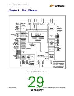
The following sections describe the functional blocks located in the LPC47M182 (see Figure 4.1). The
various Super I/O components are described in the following sections and their registers are implemented
as typical Plug-and-Play components (see section Chapter 11 − Configuration on page 167).
6.1
Super I/O Registers
Table 6.1 shows the logical device number and addresses of FDC, Serial and Parallel ports,
Keyboard/Mouse, Power Control and GPIO Block, and configuration register block of the Super I/O
immediately after power up. The logical device numbering is controlled by the LD_NUM bit in the TEST 7
configuration register (0x29. The base addresses of the blocks can be programmed via the configuration
registers. Refer to the “Configuration” section for configuration register description.
Table 6.1 – Super I/O Block Logical Device Number and Addresses
LD_NUM bit = 0 (default)
LD_NUM bit = 1
LD
LD
DEVICE
DEVICE NAME
BLOCK ADDRESS
BLOCK ADDRESS
NUMBER
NUMBER
NAME
00h
Floppy Disk
Controller
Parallel Port
Base+(0-5) and +(7)
00h
Floppy Disk
Base+(0-5) and +(7)
Controller
Base+(0-3)
01h
01h
-
-
Base+(0-7)
Base+(0-3), +(400-402)
Base+(0-7), +(400-402)
02h
03h
Serial Port 2
Serial Port 1
Base+(0-7)
Base+(0-7)
02h
03h
Serial Port 2
Parallel Port
Base+(0-7)
Base+(0-3)
Base+(0-7)
Base+(0-3), +(400-402)
Base+(0-7), +(400-402)
04h
05h
06h
07h
Power Control
Mouse
Keyboard
GPIO
Base+(0-31)
04h
05h
06h
07h
Serial Port 1
-
-
Base+(0-7)
-
-
60, 64
Base+(0-31)
Keyboard/Mou
60, 64
se
08h
09h
0Ah
-
-
-
-
-
-
08h
09h
0Ah
-
-
-
-
Runtime
Base+(0-63)
Register Block
– contains
Power Control
and GPIO
Block registers
in this mode.
-
Configuration
Base + (0-1)
-
Configuration
Base + (0-1)
SMSC LPC47M182
33
Revision 1.8 SMSC/Non-SMSC Register Sets (02-24-05)
DATASHEET

 SMSC [ SMSC CORPORATION ]