Advanced I/O Controller with Motherboard GLUE Logic
Datasheet
1=32kHz clock is not connected to the CLKI32 pin (pin is grounded).
Bit 0 controls the source of the 32kHz (nominal) clock for the nFPRST debounce circuitry, the LED blink
logic and the “wake on specific key” logic. When the external 32kHz clock is connected, that will be the
source for the nFPRST debounce circuitry, LED and “wake on specific key” logic. When the external
32kHz clock is not connected, an internal 32kHz clock source will be derived from the 14MHz clock for the
“wake on specific key” logic. The nFPRST debounce cirucitry and LED require the 32kHz clock be always
connected.
The “wake on specific key” function will not work under VTR power (VCC removed) if the external 32kHz
clock is not connected. It will work under VCC power even if the external 32 kHz clock is not connected.
5.6
5.7
14.318 MHz Clock Input
The LPC47M182 utilizes a 14.318 MHz clock input (CLOCKI). This clock is used to generate specific
clocks needed for various logic (including SIO functions, Fan Tachometer, etc.) in the LPC47M182. The
CLOCKI is powered by VCC and is not available in VTR power only (VCC=0).
Internal PWRGOOD
An internal PWRGOOD logical control is included to minimize the effects of pin-state uncertainty in the
host interface as VCC cycles on and off. When the internal PWRGOOD signal is “1” (active), VCC > 2.3V
(nominal), and the LPC47M182 host interface is active. When the internal PWRGOOD signal is “0”
(inactive), VCC <= 2.3V (nominal), and the LPC47M182 host interface is inactive; that is, LPC bus reads
and writes will not be decoded.
The LPC47M182 device pins nIO_PME, CLOCKI32, KDAT, MDAT, nRI1, nRI2, and most GPIOs (as input)
are part of the PME interface and remain active when the internal PWRGOOD signal has gone inactive,
provided VTR is powered. Other VTR powered pins listed in Table 3.1 also remain active when the
internal PWRGOOD signal has gone inactive, provided VTR is powered. See Trickle Power Functionality
section.
5.8
5.9
Maximum Current Values
See the “Operational Description” section for the maximum current values.
The maximum VTR current, ITR, is given with all outputs open (not loaded), and all inputs transitioning
from/to 0V to/from 3.3V. The total maximum current for the part is the unloaded value PLUS the maximum
current sourced by the pin that is driven by VTR. The pins that are powered by VTR are listed in the Table
3.1. The push-pull capable outputs will source minimum current specified in Table 12.2 at 2.4V when
driving.
The maximum VCC current, ICC, is given with all outputs open (not loaded) and all inputs transitioning
from/to 0V to/from 3.3V.
Power Management Events (PME/SCI)
The LPC47M182 offers support for Power Management Events (PMEs), also referred to as System
Control Interrupt (SCI) events. The terms PME and SCI are used synonymously throughout this document
to refer to the indication of an event to the chipset via the assertion of the nIO_PME output signal. See the
“PME Support” section.
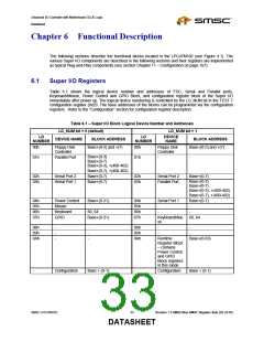
Revision 1.8 SMSC/Non-SMSC Register Sets (02-24-05)
32
SMSC LPC47M182
DATASHEET

 SMSC [ SMSC CORPORATION ]