Advanced I/O Controller with Motherboard GLUE Logic
Datasheet
5.3.1 Trickle Power Functionality
When the LPC47M182 is running under VTR only (VCC removed), PME wakeup events are active and (if
enabled) able to assert the nIO_PME pin active low. The following lists the wakeup events:
UART1 and UART 2 Ring Indicator
Keyboard data
Mouse data
“Wake on Specific Key” Logic
GPIOs for wakeup. See below.
The following requirements apply to all I/O pins that are specified to be 5 volt tolerant.
I/O buffers that are wake-up event compatible are powered by VCC. Under VTR power (VCC=0), these
pins may only be configured as inputs. These pins have input buffers into the wakeup logic that are
powered by VTR.
I/O buffers that may be configured as either push-pull or open drain under VTR power (VCC=0), are
powered by VTR. This means, at a minimum, they will source their specified current from VTR even when
VCC is present.
The GPIOs that are used for PME wakeup as input are GP10-GP17 and GP20-GP23
Buffers are powered by VTR. These pins have input buffers into the wakeup logic that are powered by
VTR. GP24 does not have input buffer into the wakeup logic.
The output buffer of GP24 is by VTR but does this pin does not have an input buffer into wakeup logic
powered by VTR.
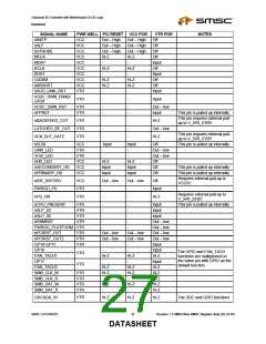
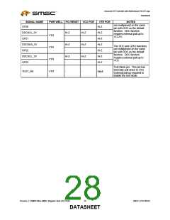
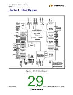
For blocks, registers and pins that are powered by VTR see Table 3.1 and Figure 4.1.
5.4
5.5
V5P0_STBY Power
The V5P0_STBY pin is used in nRSMRST generation circuit. The V5P0_STBY, however, does not power
the nRSMRST pad.
32.768 kHz Trickle Clock Input
The LPC47M182 utilizes a 32.768 kHz trickle input to supply a clock signal for the nFPRST debounce
circuitry, LED blink and wake on specific key function.
5.5.1 Indication of 32KHZ Clock
There is a bit to indicate whether or not the 32kHz clock input is connected to the LPC47M182. This bit is
located at bit 0 of the CLOCKI32 configuration register at 0xF0 in the Power Control Logical Device (when
LD_NUM=0) or Runtime Register Block Logical Device (when LD_NUM=1). This register is powered by
VTR and reset on a VTR POR.
Bit[0] (CLK32_PRSN) is defined as follows:
0=32kHz clock is connected to the CLKI32 pin (default)
SMSC LPC47M182
31
Revision 1.8 SMSC/Non-SMSC Register Sets (02-24-05)
DATASHEET

 SMSC [ SMSC CORPORATION ]