Advanced I/O Controller with Motherboard GLUE Logic
Datasheet
6.2
6.3
Host Processor Interface (LPC)
The host processor communicates with the LPC47M182 through a series of read/write registers via the
LPC interface. The port addresses for these registers are shown in Table 6.1. Register access is
accomplished through I/O cycles or DMA transfers. All registers are 8 bits wide.
LPC Interface
The following sub-sections specify the implementation of the LPC bus.
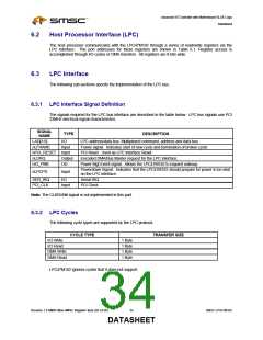
6.3.1 LPC Interface Signal Definition
The signals required for the LPC bus interface are described in the table below. LPC bus signals use PCI
33MHz electrical signal characteristics.
SIGNAL
TYPE
I/O
Input
DESCRIPTION
NAME
LAD[3:0]
LPC address/data bus. Multiplexed command, address and data bus.
Frame signal. Indicates start of new cycle and termination of broken cycle
PCI Reset. Used as LPC Interface Reset.
nLFRAME
nPCI_RESET Input
nLDRQ
Output
Encoded DMA/Bus Master request for the LPC interface.
nIO_PME
OD
Power Mgt Event signal. Allows the LPC47M182 to request wakeup.
Powerdown Signal. Indicates that the LPC47M182 should prepare for power to be shut
on the LPC interface.
Serial IRQ.
PCI Clock.
nLPCPD
Input
SER_IRQ
PCI_CLK
I/O
Input
Note: The CLKRUN# signal is not implemented in this part.
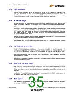
6.3.2 LPC Cycles
The following cycle types are supported by the LPC protocol.
CYCLE TYPE
TRANSFER SIZE
I/O Write
I/O Read
DMA Write
DMA Read
1 Byte
1 Byte
1 Byte
1 Byte
LPC47M182 ignores cycles that it does not support.
Revision 1.8 SMSC/Non-SMSC Register Sets (02-24-05)
34
SMSC LPC47M182
DATASHEET

 SMSC [ SMSC CORPORATION ]