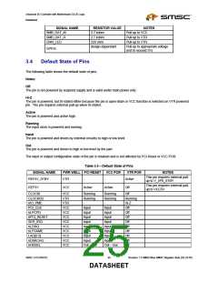
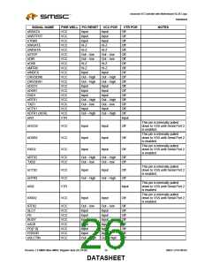
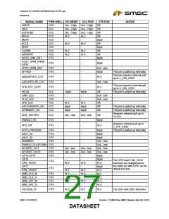
Advanced I/O Controller with Motherboard GLUE Logic
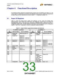
Datasheet
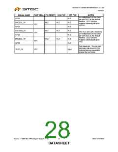
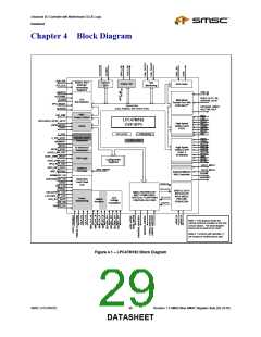
Chapter 4 Block Diagram
SER_IRQ
SERIAL IRQ /
Interrupt
CLOCK
GEN
FAN
Power LED
XOR-Chain
PCI_CLK
Monitoring
Generating
Registers
LAD[3:0]
nLFRAME
nLDRQ
PD[7:0]
BUSY, SLCT, PE,
nERROR, nACK
LPC
Multi-Mode
Parallel Port with
ChiProtectTM
Bus Interface
nPCI_RESET
nLPCPD
Internal Bus
nSTROBE, nINITP,
nSLCTIN, nALF
(Data, Address, and Control lines)
PME /
nIO_PME
RXD
Power Control
TXD
LPC47M182
(128 QFP)
GP10-GP15, GP16*, GP17*
nCTS
nRTS
nDSR
nDTR*
nDCD
nRI
High-Speed
16550A UART
PORT
(GP20-GP23)*
GP24*
GPIOs
F_CAP
VCC (3.3V)
VTR (3.3V)
Resume Reset
Generation
V_5P0_STBY
nRSMRST
REF5V
REF5V_STBY
RXD2
V_5P0_STBY
TXD2
nCTS2
nRTS2
nDSR2
nDTR2
nDCD2
nRI2
High-Speed
16550A UART
PORT 2
5V Reference
Generation
nAUD_LINK_RST
nCDC_DWN_ENAB*
W/ Infrared
CNR Logic
IRRX2
IRTX2
Configuration
Registers
nCDC_DWN_RST
nPCI_RST_OUT
nPCI_RST_OUT2
nIDE_RSTDRV
KDAT, MDAT
Buffered
nPCI_RESET
KCLK, MCLK
GA20M
PCI Reset
Keyboard/Mouse
8042 Controller
nPRIMARY_HD
nKBDRST
nSECONDARY_HD
nSCSI
Hard Drive
Front Panel
LED
WDATA
nHD_LED
nFPRST
WCLOCK
DIGITAL DATA
SEPARATOR
WITH WRITE
PRECOM-
SMSC PROPRIETARY
82077 COMPATIBLE
VERTICAL FLOPPYDISK
CONTROLLER CORE
nBACKFEED_CUT
LATCHED_BF_CUT
SCK_BJT_GATE
nPS_ON
RCLOCK
RDATA
VGA
Power
SMBus
Voltage
Sequencing
PENSATION
Isolation
Translation
PWRGD_PS
Note 1: This diagram shows the
various functions available on the chip
(not pin layout). The block diagram
should not be used for pin count.
Note 2: Functions with asterisks (*)
are located on multifunctional pins.
Figure 4.1 – LPC47M182 Block Diagram
SMSC LPC47M182
29
Revision 1.8 SMSC/Non-SMSC Register Sets (02-24-05)
DATASHEET

 SMSC [ SMSC CORPORATION ]