Advanced I/O Controller with Motherboard GLUE Logic
Datasheet
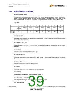
6.3.3 Field Definitions
The data transfers are based on specific fields that are used in various combinations, depending on the
cycle type. These fields are driven onto the LAD[3:0] signal lines to communicate address, control and
data information over the LPC bus between the host and the LPC47M182. See the Low Pin Count (LPC)
Interface Specification Revision 1.0 from Intel, Section 4.2 for definition of these fields.
6.3.4 NLFRAME Usage
nLFRAME is used by the host to indicate the start of cycles and the termination of cycles due to an abort
or time-out condition. This signal is to be used by the LPC47M182 to know when to monitor the bus for a
cycle.
This signal is used as a general notification that the LAD[3:0] lines contain information relative to the start
or stop of a cycle, and that the LPC47M182 monitors the bus to determine whether the cycle is intended
for it. The use of nLFRAME allows the LPC47M182 to enter a lower power state internally. There is no
need for the LPC47M182 to monitor the bus when it is inactive, so it can decouple its state machines from
the bus, and internally gate its clocks.
When the LPC47M182 samples nLFRAME active, it immediately stops driving the LAD[3:0] signal lines on
the next clock and monitor the bus for new cycle information.
The nLFRAME signal functions as described in the Low Pin Count (LPC) Interface Specification, Revision
1.0.
6.3.5
I/O Read and Write Cycles
The LPC47M182 is the target for I/O cycles. I/O cycles are initiated by the host for register or FIFO
accesses, and will generally have minimal Sync times. The minimum number of wait-states between bytes
is 1. EPP cycles will depend on the speed of the external device, and may have much longer Sync times.
Data transfers are assumed to be exactly 1-byte. If the CPU requested a 16 or 32-bit transfer, the host will
break it up into 8-bit transfers.
See the “Low Pin Count (LPC) Interface Specification” Reference, Section 5.2, for the sequence of cycles
for the I/O Read and Write cycles.
6.3.6 DMA Read and Write Cycles
DMA read cycles involve the transfer of data from the host (main memory) to the LPC47M182. DMA write
cycles involve the transfer of data from the LPC47M182 to the host (main memory). Data will be coming
from or going to a FIFO and will have minimal Sync times. Data transfers to/from the LPC47M182 are 1, 2
or 4 bytes.
See the “Low Pin Count (LPC) Interface Specification” Reference, Section 6.4, for the field definitions and
the sequence of the DMA Read and Write cycles.
6.3.7 DMA Protocol
DMA on the LPC bus is handled through the use of the nLDRQ lines from the LPC47M182 and special
encodings on LAD[3:0] from the host.
SMSC LPC47M182
35
Revision 1.8 SMSC/Non-SMSC Register Sets (02-24-05)
DATASHEET

 SMSC [ SMSC CORPORATION ]