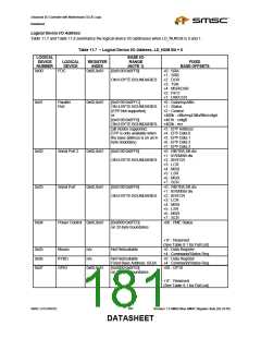
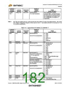
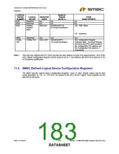
Advanced I/O Controller with Motherboard GLUE Logic
Datasheet
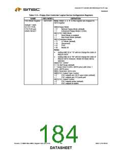
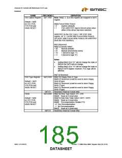
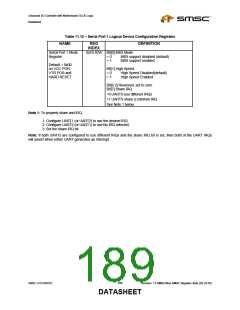
NAME
REG INDEX
DEFINITION
0xF1 R/W Note: Bits[0, 2, 3] in this register are mapped to 0xF8
register.
FDD Option Register
Default = 0x00
on VCC POR,
VTR POR and
HARD RESET
Bit[0] Forced Write Protect
= 0
= 1
Inactive (default)
FDD nWRTPRT input is forced active when
either of the drives has been selected.
nWRTPRT (to the FDC Core) = WP (FDC SRA
register, bit 1) = (nDS0 AND Forced Write Protect)
OR (nDS1 AND Forced Write Protect) OR nWRTPRT
(from the FDD Interface)
Bit[1] Reserved
Bits[3:2] Density Select
= 00
= 01
= 10
= 11
Normal (default)
Normal (reserved for users)
1 (forced to logic “1”)
0 (forced to logic “0”)
Notes:
•
Setting Bits[3:2] to “01” will not change the state of
Bit[5] in the 0xF8 will not change.
•
Setting Bits[3:2] to “10” will not change the state of
Bit[5] in 0xF8 register; however, FDC logic will be
affected.
Bit[7:4] Reserved.
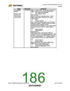
FDD Type Register
0xF2 R/W Bits[1:0] Floppy Drive A Type
Bits[3:2] Reserved (could be used to store Floppy
Default = 0xFF
on VCC POR,
VTR POR and
HARD RESET
Drive B type)
Bits[5:4] Reserved (could be used to store Floppy
Drive C type)
Bits[7:6] Reserved (could be used to store Floppy
Drive D type)
0xF3 R
Reserved, Read as 0 (read only)
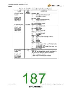
FDD0
0xF4 R/W Bits[1:0] Drive Type Select: DT1, DT0
Bits[2] Read as 0 (read only)
Default = 0x00
on VCC POR,
VTR POR and
HARD RESET
Bits[4:3] Data Rate Table Select: DRT1, DRT0
Bits[5] Read as 0 (read only)
Bits[6] Precompensation Disable PTS
=0 Use Precompensation
=1 No Precompensation
Bits[7] Read as 0 (read only)
0xF5 R
Reserved, Read as 0 (read only)
SMSC LPC47M182
185
Revision 1.8 SMSC/Non-SMSC Register Sets (02-24-05)
DATASHEET

 SMSC [ SMSC CORPORATION ]