Advanced I/O Controller with Motherboard GLUE Logic
Datasheet
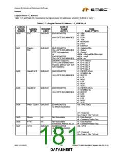
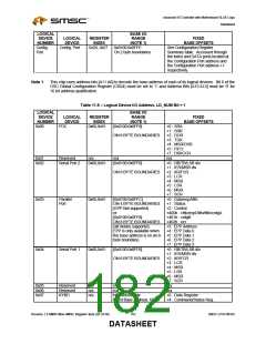
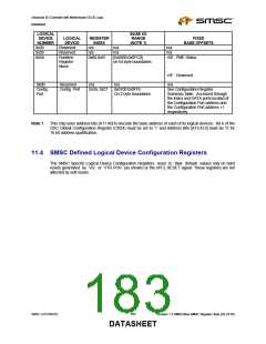
LOGICAL
BASE I/O
RANGE
DEVICE
NUMBER
0x08
LOGICAL
DEVICE
REGISTER
INDEX
n/a
FIXED
(NOTE 1)
BASE OFFSETS
Reserved
n/a
n/a
n/a
n/a
0x09
0x0A
Reserved
Runtime
Register
Block
n/a
0x60,0x61
[0x0000:0x0FC0]
+00 : PME Status
on 64-byte boundaries
.
.
.
+3F : Reserved
0x0B
Config.
Port
Reserved
n/a
n/a
n/a
Config. Port
0x26, 0x27
0x0100:0x0FFE
On 2 byte boundaries
See Configuration Register
Summary table. Accessed through
the index and DATA ports located at
the Configuration Port address and
the Configuration Port address +1
respectively.
Note 1: This chip uses address bits [A11:A0] to decode the base address of each of its logical devices. Bit 6 of the
OSC Global Configuration Register (CR24) must be set to ‘1’ and Address Bits [A15:A12] must be ‘0’ for
16 bit address qualification.
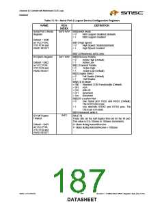
11.4 SMSC Defined Logical Device Configuration Registers
The SMSC Specific Logical Device Configuration Registers reset to their default values only on hard
resets generated by Vcc or VTR POR (as shown) or the nPCI_RESET signal. These registers are not
affected by soft resets.
SMSC LPC47M182
183
Revision 1.8 SMSC/Non-SMSC Register Sets (02-24-05)
DATASHEET

 SMSC [ SMSC CORPORATION ]