Advanced I/O Controller with Motherboard GLUE Logic
Datasheet
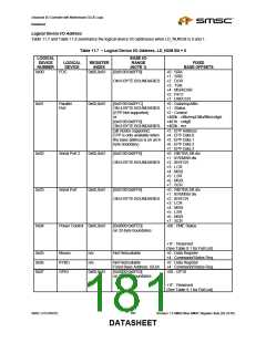
LOGICAL
DEVICE
NUMBER
Config.
BASE I/O
RANGE
LOGICAL
DEVICE
REGISTER
INDEX
FIXED
(NOTE 1)
BASE OFFSETS
Config. Port
0x26, 0x27
0x0100:0x0FFE
See Configuration Register
Summary table. Accessed through
the index and DATA ports located at
the Configuration Port address and
the Configuration Port address +1
respectively.
Port
On 2 byte boundaries
Note 1: This chip uses address bits [A11:A0] to decode the base address of each of its logical devices. Bit 6 of the
OSC Global Configuration Register (CR24) must be set to ‘1’ and Address Bits [A15:A12] must be ‘0’ for
16 bit address qualification.
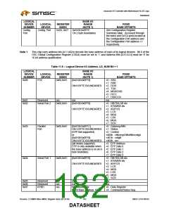
Table 11.8 – Logical Device I/O Address, LD_NUM Bit = 1
LOGICAL
DEVICE
NUMBER
0x00
BASE I/O
RANGE
LOGICAL
DEVICE
REGISTER
INDEX
FIXED
(NOTE 1)
BASE OFFSETS
FDC
0x60,0x61
[0x0100:0x0FF8]
+0 : SRA
+1 : SRB
+2 : DOR
+3 : TSR
ON 8 BYTE BOUNDARIES
+4 : MSR/DSR
+5 : FIFO
+7 : DIR/CCR
n/a
0x01
0x02
Reserved
Serial Port 2
n/a
0x60,0x61
n/a
[0x0100:0x0FF8]
+0 : RB/TB/LSB div
+1 : IER/MSB div
+2 : IIR/FCR
+3 : LCR
ON 8 BYTE BOUNDARIES
+4 : MSR
+5 : LSR
+6 : MSR
+7 : SCR
0x03
0x04
Parallel
Port
0x60,0x61
0x60,0x61
[0x0100:0x0FFC]
+0 : Data/ecpAfifo
+1 : Status
ON 4 BYTE BOUNDARIES
(EPP Not supported)
or
+2 : Control
+400h : cfifo/ecpDfifo/tfifo/cnfgA
+401h : cnfgB
+402h : ecr
[0x0100:0x0FF8]
ON 8 BYTE BOUNDARIES
(all modes supported,
EPP is only available when
+3 : EPP Address
+4 : EPP Data 0
the base address is on an 8- +5 : EPP Data 1
byte boundary)
+6 : EPP Data 2
+7 : EPP Data 3
+0 : RB/TB/LSB div
+1 : IER/MSB div
+2 : IIR/FCR
+3 : LCR
Serial Port 1
[0x0100:0x0FF8]
ON 8 BYTE BOUNDARIES
+4 : MSR
+5 : LSR
+6 : MSR
+7 : SCR
0x05
0x06
0x07
Reserved
Reserved
KYBD
n/a
n/a
n/a
n/a
n/a
n/a
n/a
Not Relocatable
Fixed Base Address: 60,64
+0 : Data Register
+4 : Command/Status Reg.
Revision 1.8 SMSC/Non-SMSC Register Sets (02-24-05)
182
SMSC LPC47M182
DATASHEET

 SMSC [ SMSC CORPORATION ]