Advanced I/O Controller with Motherboard GLUE Logic
Datasheet
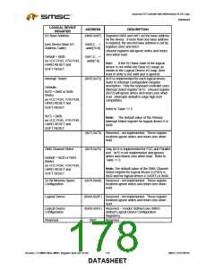
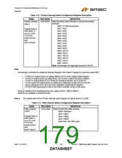
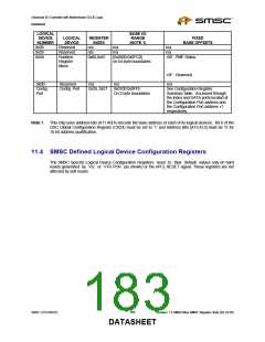
Table 11.5 – Primary Interrupt Select Configuration Register Description
NAME
Primary Interrupt
Select
REG INDEX
DEFINITION
0x70 (R/W) Bits[3:0] selects which interrupt is used for the primary
Interrupt.
0x00= no interrupt selected
0x01= IRQ1
Default=0x00 or
0x06 (Note 1)
0x02= IRQ2
on VCC POR,
0x03= IRQ3
VTR POR,
0x04= IRQ4
HARD RESET
and
0x05= IRQ5
0x06= IRQ6
SOFT RESET
0x07= IRQ7
0x08= IRQ8
0x09= IRQ9
0x0A= IRQ10
0x0B= IRQ11
0x0C= IRQ12
0x0D= IRQ13
0x0E= IRQ14
0x0F= IRQ15
Note: All interrupts are edge high (except ECP/EPP)
Note:
An Interrupt is activated by setting the Interrupt Request Level Select 0 register to a non-zero value AND:
For the FDC logical device by setting DMAEN, bit D3 of the Digital Output Register.
For the PP logical device by setting IRQE, bit D4 of the Control Port and in addition
For the PP logical device in ECP mode by clearing serviceIntr, bit D2 of the ecr.
For the Serial Port logical device by setting any combination of bits D0-D3 in the IER
and by setting the OUT2 bit in the UART's Modem Control (MCR) Register.
For the KYBD logical device (refer to the KYBD controller section of this spec).
IRQs are disabled if not used/selected by any Logical Device. Refer to Note A.
All IRQ’s are available in Serial IRQ mode.
Note 1: The default value of the Primary Interrupt Select register for logical device 0 is 0x06.
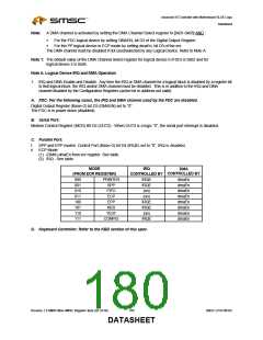
Table 11.6 – DMA Channel Select Configuration Register Description
NAME
REG INDEX
0x74 (R/W)
DEFINITION
Bits[2:0] select the DMA Channel.
0x00= Reserved
DMA Channel
Select
0x01= DMA1
Default=0x02 or
0x04 (Note 1)
0x02= DMA2
0x03= DMA3
0x04-0x07= No DMA active
on VCC POR,
VTR POR,
HARD RESET
and
SOFT RESET
SMSC LPC47M182
179
Revision 1.8 SMSC/Non-SMSC Register Sets (02-24-05)
DATASHEET

 SMSC [ SMSC CORPORATION ]