Advanced I/O Controller with Motherboard GLUE Logic
Datasheet
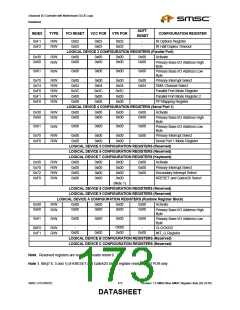
REGISTER
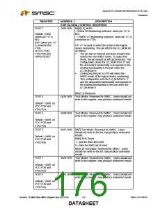
TEST 3
ADDRESS
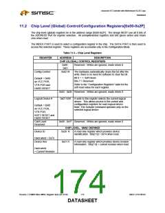
CHIP (GLOBAL) CONTROL REGISTERS
0x2F R/W Test Modes: Reserved for SMSC. Users should not
write to this register, may produce undesired results.
DESCRIPTION
Default = 0x00, on
VCC POR and
VTR POR
Note 1: To allow the selection of the configuration address to a user defined location, these Configuration Address
Bytes are used. There is no restriction on the address chosen, except that A0 is 0, that is, the address
must be on an even byte boundary. As soon as both bytes are changed, the configuration space is moved
to the specified location with no delay (Note: Write byte 0, then byte 1; writing CR27 changes the base
address).
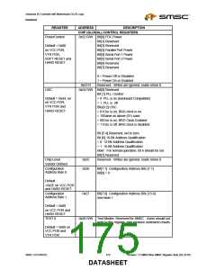
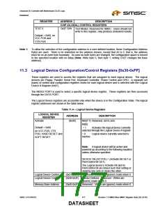
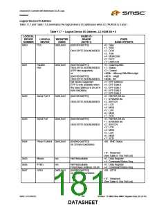
11.3 Logical Device Configuration/Control Registers [0x30-0xFF]
These registers are used to access the registers that are assigned to each logical device. The logical
devices are Floppy, Parallel, Serial Port, Keyboard Controller, Power Control and GPIO. A separate set
(bank) of control and configuration registers exists for each logical device and is selected with the Logical
Device # Register (0x07).
The INDEX PORT is used to select a specific logical device register. These registers are then accessed
through the DATA PORT.
The Logical Device registers are accessible only when the device is in the Configuration State. The logical
register addresses are shown in the table below.
Table 11.4 – Logical Device Registers
LOGICAL DEVICE
ADDRESS
DESCRIPTION
REGISTER
Activate
(0x30)
Bits[7:1] Reserved, set to zero.
Bit[0]
Default = 0x00
= 1
Activates the logical device currently
selected through the Logical Device # register.
on VCC POR, VTR
POR, HARD RESET and
= 0
Logical device currently selected is
inactive
SOFT RESET
Note: A logical device will be active and
powered up according to the following equation
unless otherwise specified:
DEVICE ON (ACTIVE) = (Activate Bit SET or
Pwr/Control Bit SET).
The Logical device’s Activate Bit and its
Pwr/Control Bit are linked such that setting or
clearing one sets or clears the other.
Logical Device Control
Logical Device Control
(0x31-0x37) Reserved – Writes are ignored, reads return 0.
(0x38-0x3F) Vendor Defined - Reserved - Writes are
ignored, reads return 0.
Memory Base Address
(0x40-0x5F) Reserved – Writes are ignored, reads return 0.
SMSC LPC47M182
177
Revision 1.8 SMSC/Non-SMSC Register Sets (02-24-05)
DATASHEET

 SMSC [ SMSC CORPORATION ]