Advanced I/O Controller with Motherboard GLUE Logic
Datasheet
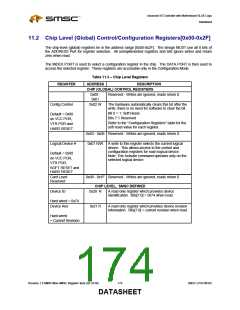
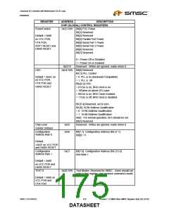
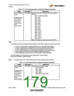
REGISTER
ADDRESS
CHIP (GLOBAL) CONTROL REGISTERS
DESCRIPTION
PowerControl
0x22 R/W Bit[0] FDC Power
Bit[1] Reserved
Default = 0x00
on VCC POR,
VTR POR,
Bit[2] Reserved
Bit[3] Parallel Port Power
Bit[4] Serial Port 1 Power
Bit[5] Serial Port 2 Power
Bit[6] Reserved
SOFT RESET and
HARD RESET
Bit[7] Reserved
0 = Power Off or Disabled
1 = Power On or Enabled
Reserved - Writes are ignored, reads return 0.
0x23 R
OSC
0x24 R/W Bit[0] Reserved
Bit [1] PLL Control
Default = 0x44, on
on VCC POR,
VTR POR and
HARD RESET
= 0 PLL is on (backward Compatible)
= 1 PLL is off
Bits[3:2] OSC
= 01Osc is on, BRG clock is on.
= 10Same as above (01) case.
= 00Osc is on, BRG Clock Enabled.
= 11Osc is off, BRG clock is disabled.
Bit [5:4] Reserved, set to zero
Bit [6] 16-Bit Address Qualification
= 0 12-Bit Address Qualification
= 1 16-Bit Address Qualification
Note: For normal operation, bit 6 should be set.
Bit[7] Reserved
Chip Level
0x25
0x26
Reserved - Writes are ignored, reads return 0.
Vendor Defined
Configuration
Bit[7:1] Configuration Address Bits [7:1]
Bit[0] = 0
Address Byte 0
Default
=0x2E on VCC POR
and HARD RESET
Configuration
0x27
Bit[7:0] Configuration Address Bits [15:8]
See Note 1
Address Byte 1
Default = 0x00
on VCC POR and
HARD RESET
TEST 8
0x28 R/W Test Modes: Reserved for SMSC. Users should not
write to this register, may produce undesired results.
Default = 0x00 on
VCC POR and
VTR POR
SMSC LPC47M182
175
Revision 1.8 SMSC/Non-SMSC Register Sets (02-24-05)
DATASHEET

 SMSC [ SMSC CORPORATION ]