Advanced I/O Controller with Motherboard GLUE Logic
Datasheet
Table 7.38 – nPS_ON Truth Table
INPUTS
NCPU_PRESENT
OUTPUT
nPS_ON
Hi-Z
NSLP_S3
0
0
1
1
0
1
0
1
0
Hi-Z
Hi-Z
See Table 13.3 for nPS_ON timing.
7.37 PWRGD_PLATFORM Logic
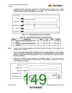
Currently the two signals available for power sequencing control (BF_CUT & LATCHED_BF_CUT) occur
~1ms before nPCI_RESET de-assertion. An option is required to insert more delay from ACPI power
sequencing events to software runtime. To do this, the PWRGD_3V signal, needs to be redefined as
PWRGD_PLATFORM. The assertion and de-assertion edge is described below, and is summarized in
Table 7.39 – PWRGD_PLATFORM Truth Table.
Negative edge (S0->S3/S5): The 1-0 transition of nSLP_S3 input or the 1-0 transition (or 0 level) of
PWRGD_PS input would cause an immediate 1-0 transition (or 0 level) of PWRGD_PLATFORM.
Positive edge (S3/S5->S0): The 0-1 transition of PWRGD_PS input would cause a 0-1 transition of
PWRGD_3V. The PWRGD_3V transition is either immediate (no delay) or after a 100ms (min) to
120ms (max) delay from the 0-1 transition of PWRGD_PS.
The delay is optional and will be governed by a lockable select bit in the nIO_PME register (located at
offset 16h in the in the Power Control Logical Device, when LD_NUM=0, or Runtime Register Block
Logical Device, when LD_NUM=1). Default operation selects the delay. An internal delay counter is used
to determine whether the 100-120 msec delay time has elapsed.
Table 7.39 – PWRGD_PLATFORM Truth Table
INTERNAL DELAY
ELAPSED?
0 = NO
PWRGD_PLATFO
PWRGD_PLATFO
RM
NSLP_S3
PWRGD_PS
RM SELECT BIT
1= YES
1-0 transition or 0
level
X
X
X
0
1-0 transition or 0
level
0-1 transition
X
1
1
X
0
1
X
X
0
0
1 (no delay)
0 (delay time not
0-1 transition
elapsed)
1 (after 100-120 msec
delay)
1
0-1 transition
1
1
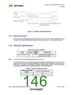
A timing diagram for generating the PWRGD_PLATFORM is shown below:
SMSC LPC47M182
145
Revision 1.8 SMSC/Non-SMSC Register Sets (02-24-05)
DATASHEET

 SMSC [ SMSC CORPORATION ]