Advanced I/O Controller with Motherboard GLUE Logic
Datasheet
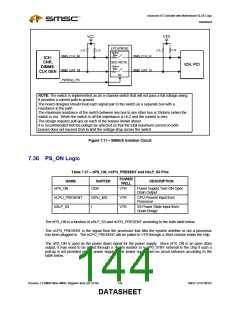
VCC
VTR
LPC47M182
2.7k
2.7k
2.7k
2.7k
25ohm
Max
SMB_CLK_M
SMB_CLK_R
SMB_DAT_R
ICH,
CNR,
SEE NOTE
ICH, PCI
25ohm
DIMMS,
CLK GEN
Max
SMB_DAT_M
PWRGD_PS
EN
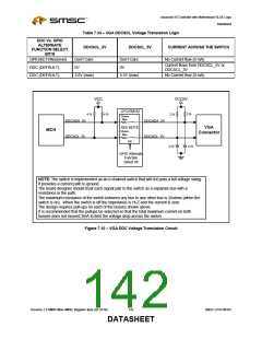
NOTE: The switch is implemented as an n-channel switch that will not pass a full voltage swing.
It provides a current path to ground.
The board designer should treat each signal pair to the switch as a separate bus with a
resistance in the path.
The maximum resistance of the switch between any bus to any other bus is 25ohms (when the
switch is on). When the switch is off the impedance is Hi-Z and the current is zero.
The design requires pull-ups on each of the busses shown above.
It is recommended that the pullups be selected so that the total maximum current on both
busses does not exceed 2mA to limit the voltage drop across the switch.
Figure 7.11 – SMBUS Isolation Circuit
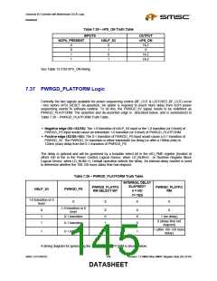
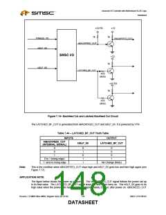
7.36 PS_ON Logic
Table 7.37 – nPS_ON, nCPU_PRESENT and nSLP_S3 Pins
POWER
NAME
nPS_ON
BUFFER
DESCRIPTION
WELL
VTR
OD8
Power Supply Turn-ON Open
Drain Output
nCPU_PRESENT
nSLP_S3
ISPU_400
I
VTR
VTR
CPU Present Input from
Processor
S3 Power State Input from
South Bridge
The nPS_ON is a function of nSLP_S3 and nCPU_PRESENT according to the truth table below.
The nCPU_PRESENT is the signal from the processor that tells the system whether or not a processor
has been plugged in. The nCPU_PRESENT will be pulled to VTR through a 30uA resistor inside the chip.
The nPS_ON is used as the power down signal for the power supply. Since nPS_ON is an open drain
output, it may need to be pulled through a 1kohm resistor to V_5P0_STBY external to the chip if such a
pull-up is not provided on the power supply. The power supply turn-on circuit behaves according to the
table below.
Revision 1.8 SMSC/Non-SMSC Register Sets (02-24-05)
144
SMSC LPC47M182
DATASHEET

 SMSC [ SMSC CORPORATION ]