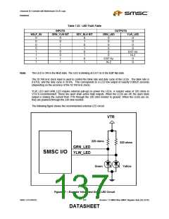
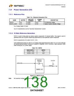
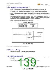
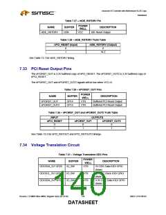
Advanced I/O Controller with Motherboard GLUE Logic
Datasheet
POWER
WELL
VTR
NAME
BUFFER
DESCRIPTION
DDCSCL_3V/ GP23
IO_SW
3.3V DDC Clock IOD/ GPIO
(Note)
Note:
The DDC_5V signals require external pull-up to VCC5V. The DDC_3V signals require external pull-up to
VCC. If DDC functions are selected on the pins, the pins will tri-state when VCC is removed.
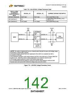
The VGA DDC voltage translation circuitry is used in conjunction with integrated VGA chipsets. Since the
chipset operates at 3.3V signal levels and the VGA signals are specified at 5V signal levels, on-board
voltage translation is needed for the DDC signals. This is a non-inverting translation. See the Table 7.32
and Table 7.33 for further details on the logic.
The DDC data pins and the DDC clock pins function as inputs shorted together through the isolation
resistor. The DDC signals require external pull-up resistors on LPC47M182. See the “Pins That Require
External Resistors” section for resistor values. See Figure 7.10 for recommended schematic
implementation. Note the switch is always on after the DDC functions are selected on the GPIO pins. That
is, the switch is controlled by the GPIO alternate function select bits. Once the DDC functions are
selected, the switch is closed and remains closed when VCC is removed. The current flow is controlled by
the external signals on the DDC pins. See the tables below for the current flow across the switch based
on the voltage levels on the pins. The switch provides a 25ohm resistance to ground.
This circuit requires ESD protection external to the chip to protect the device from hot-plugging on the VGA
connector. See the “Electrical Characteristics” section for current and voltage requirements.
Due to the multiplexing with GPIO pins, these pins are powered by VTR. (Without the multiplexing
requirement, these pins could be powered by VCC).
Note:
If any of the Alternate Function Select bits in GP20 to GP23 registers are set for DDC function, the DDC
functions will be selected on all four GP20 to GP23 pins. However, it is recommended that the DDC
functions be selected via the Alternate Function Select bits in all of the GP20 to GP23 registers when
using the DDC functions.
The GP20 to GP23 registers are defined in “GPIO Runtime Registers” section when LD_NUM=0 and
“Runtime Register Block Runtime Registers” section when LD_NUM=1.
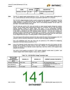
Table 7.32 – VGA DDCSDA Voltage Translation Logic
DDC VS. GPIO
ALTERNATE
FUNCTION SELECT
BIT/S
GPIO/EETI/Reserved
DDC (DEFAULT)
DDC (DEFAULT)
DDCSDA_3V
Don’t Care
DDCSDA_5V
Don’t Care
CURRENT ACROSS THE SWITCH
No Current flow (0 mA)
Current flows from DDCSDA_5V or
0V
0V
DDCSDA_3V
3.6V (max)
5.5V (max)
No Current flow (0 mA)
SMSC LPC47M182
141
Revision 1.8 SMSC/Non-SMSC Register Sets (02-24-05)
DATASHEET

 SMSC [ SMSC CORPORATION ]