Advanced I/O Controller with Motherboard GLUE Logic
Datasheet
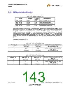
7.35 SMBus Isolation Circuitry
Table 7.34 – SMBus Isolation Pins
POWER
WELL
VTR
VTR
VTR
VTR
NAME
BUFFER
IO_SW
IO_SW
IO_SW
IO_SW
DESCRIPTION
SMB_CLK_M
SMB_DAT_M
SMB_CLK_R
SMB_DAT_R
Main Well SMBus Clock
Main Well SMBus Data
Resume Well SMBus Clock
Resume Well SMBus Data
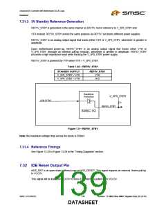
The SMBus Isolation circuitry is used to isolate the main SMBus signals from the resume SMBus signals
during power down modes. The SMB data pins and the SMB clock pins function as inputs shorted together
through the isolation resistor when the switch is closed. The SMBus signals require external pull-up
resistors on LPC47M182. See Figure 7.11 for recommended schematic implementation. The switch is
controlled by the PWRGD_PS signal. The switch is closed as long as PWRGD_PS is ‘1’. The current flow
is controlled by the external signals on the SMB pins. See Table 7.35 and Table 7.36 for the current flow
across the switch based on the voltage levels on the pins. The switch provides a 25ohm resistance to
ground.
These pins are powered by VTR.
Table 7.35 – SMB_CLK Isolation Logic
PWRGD_PS
SMB_CLK_M
Don’t Care
SMB_CLK_R
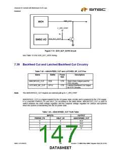
Don’t Care
CURRENT ACROSS THE SWITCH
0
No Current flow (0 mA)
Current flows from SMB_CLK_R or
1
1
0V
0V
SMB_CLK_M
3.6V (max)
3.6V (max)
No Current flow (0 mA)
Table 7.36 – SMB_DAT Isolation Logic
CURRENT DIRECTION ACROSS THE
SWITCH
PWRGD_PS
SMB_DAT_M
SMB_DAT_R
Don’t Care
0V
0
1
1
Don’t Care
0V
No Current flow (0 mA)
Current flows from SMB_DAT_R or
SMB_DAT_M
3.6V (max)
3.6V (max)
No Current flow (0 mA)
SMSC LPC47M182
143
Revision 1.8 SMSC/Non-SMSC Register Sets (02-24-05)
DATASHEET

 SMSC [ SMSC CORPORATION ]