Advanced I/O Controller with Motherboard GLUE Logic
Datasheet
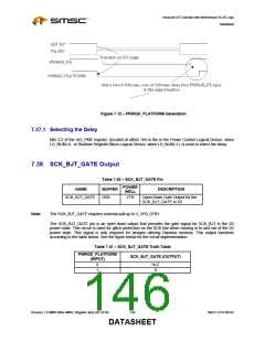
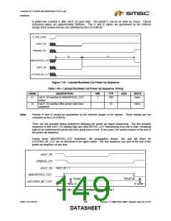
Figure 7.12 – PRWGD_PLATFORM Generation
7.37.1 Selecting the Delay
Bits 3:2 of the nIO_PME register, (located at offset 16h in the in the Power Control Logical Device, when
LD_NUM=0, or Runtime Register Block Logical Device, when LD_NUM=1), is used to select the delay.
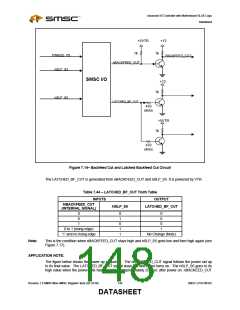
7.38 SCK_BJT_GATE Output
Table 7.40 – SCK_BJT_GATE Pin
POWER
NAME
BUFFER
DESCRIPTION
WELL
SCK_BJT_GATE
OD8
VTR
Open-Drain Gate Output for the
SCK_BJT_GATE in S3
Note:
The SCK_BJT_GATE requires external pull-up to V_5P0_STBY.
The SCK_BJT_GATE pin is an open drain output that provides the gate signal for SCK_BJT in the S3
power state. This circuit is used for glitch protection on the SCK line when moving in to and out of the S3
power state. This signal is only required for designs utilizing Rambus memory. This output functions
according to the table below. See the figure below for the circuit implementation.
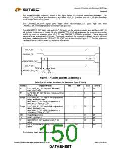
Table 7.41 – SCK_BJT_GATE Truth Table
PWRGD_PLATFORM
SCK_BJT_GATE (OUTPUT)
(INPUT)
0
1
Hi-Z
0
Revision 1.8 SMSC/Non-SMSC Register Sets (02-24-05)
146
SMSC LPC47M182
DATASHEET

 SMSC [ SMSC CORPORATION ]