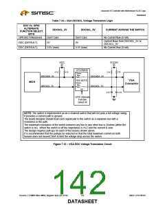
Advanced I/O Controller with Motherboard GLUE Logic
Datasheet
7.31 Power Generation (5V)
7.31.1 Reference Pins
Table 7.24 – Reference Generation Pins
MAX OUT
CURRENT
3.3mA
3.3mA
POWER
WELL
VCC
VTR
NAME
REF5V
REF5V_STBY
OAN: Analog Output, 5V level.
BUFFER
AO
AO
DESCRIPTION
5V Reference Output
Highest System Standby Voltage
See DC characteristics see the “Electrical Characteristics” section.
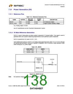
7.31.2 5V Main Reference Generation
REF5V is used to help power-up various system components’ 5V tolerant buffers. This signal is used to
guarantee there are no power sequencing requirements at each particular system component.
REF5V is powered by VCC when VCC5V < VCC.
Upon motherboard power-up, REF5V is an analog output signal that tracks either VCC or VCC5V (through
an external pull-up resistor), whichever is greater in amplitude. REF5V becomes a high impedance input
while tracking the VCC power supply.
Table 7.25 – REF5V
MAIN SUPPLY
VCC5V < VCC
VCC5V > VCC
REF5V
VCC
Hi-Z
Backdrive
Protection
VCC5V
VCC (3.3V)
1k
REF5V
SMSC I/O
Figure 7.8 – REF5V Circuit
the maximum voltage drop across the diode is 350mV.
Note:
Revision 1.8 SMSC/Non-SMSC Register Sets (02-24-05)
138
SMSC LPC47M182
DATASHEET

 SMSC [ SMSC CORPORATION ]