The parallel port logic can change powerdown modes when the ECP mode is changed through the ecr register or when
the parallel port mode is changed through the configuration registers.
6.9 Real Time Clock
The Real Time Clock Supercell (RTC) is a complete time of day clock with alarm, day of month alarm, one hundred
year calendar, a century byte, and a programmable periodic interrupt. The RTC address space consists of two-128
byte banks of CMOS RAM (Bank0 and Bank1.) Each bank is accessible via address and data ports. These access
ports have relocatable addresses and are accessible by the CPU. The 128 bytes of Bank0 contain the following:
eleven registers of time, calendar, century, and alarm data, four control and status registers, and 112 bytes of
general-purpose registers. The 128 bytes of Bank1 contain general-purpose registers.
Features:
Allow 32kHz-clock input or a 32kHz crystal.
Counts seconds, minutes, and hours of the day.
Counts days of the week, date, month and year.
Binary or BCD representation of time, calendar and alarm.
24-hour daily alarm.
30-day alarm.
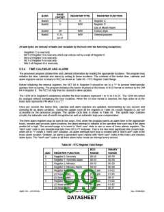
RTC/CMOS Bank Addresses are relocatable.
The RTC CMOS Bank0 index register (70h) is shadowed
RTC power source is switched internally between the VTR and VBAT pins according to VTR_PWRGD
Lockable CMOS Ram Address Ranges.
Polarity selection on IRQ8
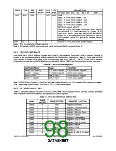
6.9.1 CONFIGURATION REGISTERS
The RTC configuration registers, in Logical Device Number 0x06, provide activation control and the base address for
the run-time registers (See Table 45)
The activate bit register 0x30, Bit D0 enables RTC/CMOS Bank0.
The activate bit register 0x30, Bit D1 enables RTC/CMOS Bank1.
Table 45 − RTC Configuration Registers
INDEX
TYPE
PCI
RESET
SOFT
RESET POR
VCC VTR
POR
0x00 0x00 Activate
RESERVED
DESCRIPTION
D4 D3 D2
D7 D6
D5
D1
D0
0x30
R/W
0x00
0x00
0x00
Activate Activate
CMOS
Bank1
RTC/
CMOS
Bank0
0x60
R/W
0x00
0x00 0x00 RTC/CMOS Bank0 Primary Base Address High Byte
“0” “0”
“0”
“0”
A1
1
A1
0
A9
A8
0x61
0x62
R/W
R/W
0x70
0x00
0x70
0x00
0x70 0x00 RTC/CMOS Bank0 Primary Base Address Low Byte
A7 A6
A5
A4
A3
A2
A1
“0” Note
0x00 0x00 CMOS Bank1 Primary Base Address High Byte
“0” “0”
“0”
“0”
A1
1
A1
0
A9
A8
0x63
0x70
R/W
R/W
0x74
0x00
0x74
0x00
0x74 0x00 CMOS Bank1 Primary Base Address Low Byte
A7 A6 A5 A4 A3 A2 A1
“0” Note
0x00 0x00 Primary Interrupt Select (Note 1)
SMSC DS – LPC47S45x
Page 97 of 259
Rev. 07/09/2001
DATASHEET

 SMSC [ SMSC CORPORATION ]