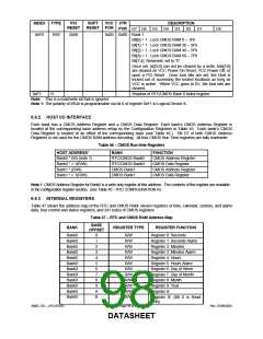
INDEX
TYPE
PCI
RESET
SOFT
RESET POR
VCC VTR
POR
0x00 0x00 Bank 1:
DESCRIPTION
D4 D3 D2
D7 D6
D5
D1
D0
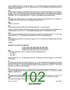
0xF0
R/W
0x00
-
Bit[0] = 1 : Lock CMOS RAM 0 – 1Fh
Bit[1] = 1 : Lock CMOS RAM 20 – 3Fh
Bit[2] = 1 : Lock CMOS RAM 40 – 5Fh
Bit[3] = 1 : Lock CMOS RAM 60 – 7Fh
Bit[7:4] Reserved, set to “0”
Once set, bit[3:0] can not be cleared by a write; bits[3:0]
are cleared on VCC Power On Reset, VCC Power Off, or
upon a PCI Reset. Once lock bits are set, the Host is
locked out of accessing the locked locations as long as
VCC is active. When VCC goes to 0V, the lock bits are
cleared.
0xF1
R
-
-
-
-
Shadow of RTC/CMOS Bank 0 Index register
Note: This is a read/write bit that is ignored.
Note 1: The polarity of IRQ8 is programmable via bit 0 of register 0xF1 in Logical Device A.
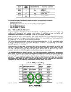
6.9.2 HOST I/O INTERFACE
Each bank has a CMOS Address Register and a CMOS Data Register. Each bank’s CMOS Address Register is
located at the corresponding base address setup by the Configuration Registers in Table 45. Each bank’s CMOS
Data Register is located at an offset of the corresponding base (see Table 46.) Bit D7 of both CMOS Address
Registers is not used for the CMOS RAM address decoding. All four CMOS Run Time registers are fully read/write.
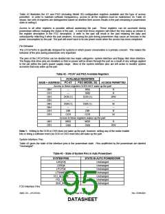
Table 46 − CMOS Run time Registers
HOST ADDRESS*
Bank0 * (W) (note 1)
Bank0 * + 1(R/W)
Bank1 * (R/W)
BANK
FUNCTION
RTC/CMOS Bank0
RTC/CMOS Bank0
CMOS Bank1
CMOS Bank1
CMOS Address Register
CMOS Data Register
CMOS Address Register
CMOS Data Register
Bank1 * + 1(R/W)
Note 1: CMOS Address Register for Bank0 is a write only register at this address. The contents of this register are readable
in the configuration register section. (see Table 45 − RTC CONFIGURATION R)
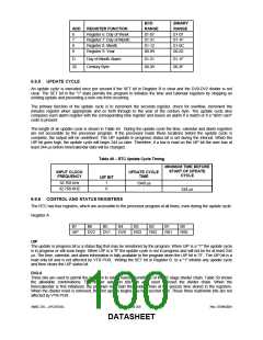
6.9.3 INTERNAL REGISTERS
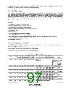
Table 47 shows the address map of the RTC and CMOS RAM, eleven registers of time, calendar, century, and alarm
data, four control and status registers, and 241 bytes of CMOS registers
Table 47 − RTC and CMOS RAM Address Map
BASE
OFFSET
BANK
REGISTER TYPE
REGISTER FUNCTION
Bank0
Bank0
Bank0
Bank0
Bank0
Bank0
Bank0
Bank0
Bank0
Bank0
Bank0
Bank0
0
1
2
3
4
5
6
7
8
9
A
B
R/W
R/W
R/W
R/W
R/W
R/W
R/W
R/W
R/W
R/W
R/W
R/W
Register 0: Seconds
Register 1: Seconds Alarm
Register 2: Minutes
Register 3: Minutes Alarm
Register 4: Hours
Register 5: Hours Alarm
Register 6: Day of Week
Register 7: Day of Month
Register 8: Month
Register 9: Year
Register A:
Register B: (Bit 0 is Read
Only)
SMSC DS – LPC47S45x
Page 98 of 259
Rev. 07/09/2001
DATASHEET

 SMSC [ SMSC CORPORATION ]