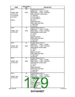
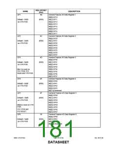
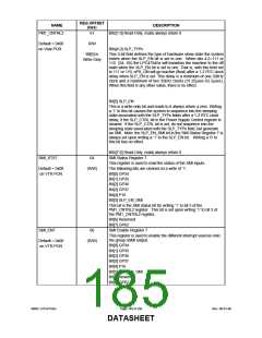
REG OFFSET
(hex)
NAME
DESCRIPTION
General Purpose I/0 Data Register 1
GP1
4B
Bit[0] GP10
Default = 0x00
on VTR POR
(R/W)
Bit[1] GP11
Bit[2] GP12
Bit[3] GP13
Bit[4] GP14
Bit[5] GP15
Bit[6] GP16
Bit[7] GP17
GP2
4C
General Purpose I/0 Data Register 2
Bit[0] GP20
Default = 0x00
on VTR POR
(R/W)
Bit[1] GP21
Bit[2] GP22
Bit[3] GP23
Bit[4] GP24
Bit[5] GP25
Bit[6] GP26
Bit[7] GP27
GP3
4D
General Purpose I/0 Data Register 3
Bit[0] GP30
Default = 0x00
on VTR POR
(R/W)
Bit[1] GP31
Bit[2] GP32
Bit[3] GP33
Bits 3 is reset on
VCC POR, PCI
Reset and VTR POR
Bit[4] GP34
Bit[5] GP35
Bit[6] GP36
Bit[7] GP37
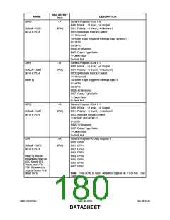
GP4
4E
General Purpose I/0 Data Register 4
Bit[0] GP40
Default = 0x00
on VTR POR
(R/W)
Bit[1] GP41
Bit[2] GP42
Bit[3] GP43
Bit[7:4] Reserved
General Purpose I/0 Data Register 5
Bit[0] GP50
GP5
4F
Default = 0x00
on VTR POR
(R/W)
Bit[1] GP51
Bit[2] GP52
Bit[3] GP53
Bit[3] is reset on VTR
POR,
Bit[4] GP54
Bit[5] GP55
VCC POR and
PCI RESET
Bit[6] GP56
Bit[7] GP57
GP6
50
General Purpose I/0 Data Register 6
Bit[0] GP60
Default = 0x00
on VTR POR
(R/W)
Bit[1] GP61
Bit[2] GP62
Bit[7-3] Reserved
SMSC LPC47S45x
Page 181 of 259
Rev. 06-01-06
DATASHEET

 SMSC [ SMSC CORPORATION ]