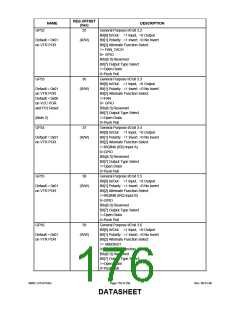
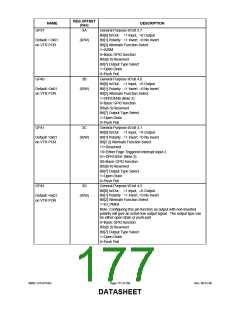
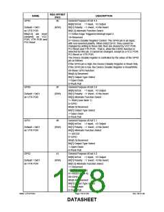
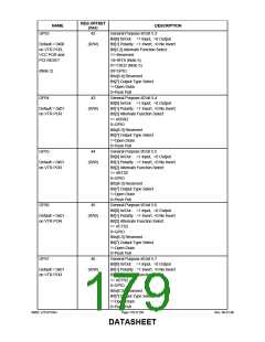
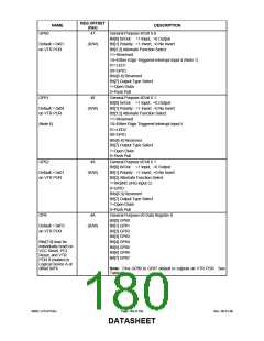
REG OFFSET
(hex)
NAME
DESCRIPTION
General Purpose I/0 bit 6.0
GP60
47
Bit[0] In/Out : =1 Input, =0 Output
Bit[1] Polarity : =1 Invert, =0 No Invert
Bit[3:2] Alternate Function Select
11=Reserved
Default = 0x01
on VTR POR
(R/W)
10=Either Edge Triggered Interrupt Input 4 (Note 1)
01=LED1
00=GPIO
Bits[6:4] Reserved
Bit[7] Output Type Select
1=Open Drain
0=Push Pull
GP61
48
General Purpose I/0 bit 6.1
Bit[0] In/Out : =1 Input, =0 Output
Bit[1] Polarity : =1 Invert, =0 No Invert
Bit[3:2] Alternate Function Select
11=Reserved
Default = 0x04
on VTR POR
(R/W)
(Note 6)
10=Either Edge Triggered Interrupt Input 5
01=LED2
00=GPIO
Bits[6:4] Reserved
Bit[7] Output Type Select
1=Open Drain
0=Push Pull
GP62
49
General Purpose I/0 bit 6.1
Bit[0] In/Out : =1 Input, =0 Output
Bit[1] Polarity : =1 Invert, =0 No Invert
Bit[2] Alternate Function Select
1=IRQINC (IRQ Input C)
0=GPIO
Default = 0x01
on VTR POR
(R/W)
Bits[6:3] Reserved
Bit[7] Output Type Select
1=Open Drain
0=Push Pull
GP8
4A
General Purpose I/0 Data Register 8
Bit[0] GP80
Default = 0xF0
on VTR POR
(R/W)
Bit[1] GP81
Bit[2] GP82
Bit[3] GP83
Bits[7:0] may be
individually reset on
VCC Reset, PCI
Reset, and VTR
POR if enabled in
Logical Device A at
offset 0xF6
Bit[4] GP84
Bit[5] GP85
Bit[6] GP86
Bit[7] GP87
Note: Pins GP80 to GP87 default to outputs on VTR POR. See
Table 94.
SMSC LPC47S45x
Page 180 of 259
Rev. 06-01-06
DATASHEET

 SMSC [ SMSC CORPORATION ]