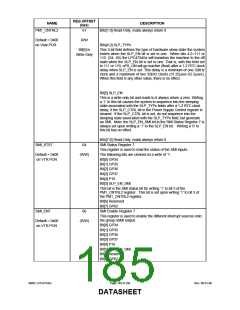
REG OFFSET
(hex)
NAME
DESCRIPTION
PM1_CNTRL2
61
Bits[1:0] Read-Only, reads always return 0
Default = 0x00
on Vbat POR
R/W
Bits[4:2] SLP_TYPx
Bit[5] is
Write-Only
This 3-bit field defines the type of hardware sleep state the system
enters when the SLP_EN bit is set to one. When bits 4:2=111 or
110 (S4, S5) the LPC47S45x will transition the machine to the off
state when the SLP_EN bit is set to one. That is, with this field set
to 111 or 110, nPS_ON will go inactive (float) after a 1-2 RTC clock
delay when SLP_EN is set. This delay is a minimum of one 32kHz
clock and a maximum of two 32kHz clocks (31.25μsec-62.5μsec).
When this field is any other value, there is no effect.
Bit[5] SLP_EN
This is a write-only bit and reads to it always return a zero. Writing
a ‘1’ to this bit causes the system to sequence into the sleeping
state associated with the SLP_TYPx fields after a 1-2 RTC clock
delay, if the SLP_CTRL bit in the Power Supply Control register is
cleared. If the SLP_CTRL bit is set, do not sequence into the
sleeping state associated with the SLP_TYPx field, but generate
an SMI. Note: the SLP_EN_SMI bit in the SMI Status Register 7 is
always set upon writing a ‘1’ to the SLP_EN bit. Writing a ‘0’ to
this bit has no effect.
Bits[7:6] Read-Only, reads always return 0
SMI_STS7
64
SMI Status Register 7
This register is used to read the status of the SMI inputs.
Default = 0x00
on VTR POR
(R/W)
The following bits are cleared on a write of ‘1’.
Bit[0] GP34
Bit[1] GP35
Bit[2] GP36
Bit[3] GP37
Bit[4] P16
Bit[5] SLP_EN_SMI
This bit is the SMI status bit for writing ‘1’ to bit 5 of the
PM1_CNTRL2 register. This bit is set upon writing ‘1’ to bit 5 of
the PM1_CNTRL2 register.
Bit[6] Reserved
Bit[7] GP62
SMI_EN7
66
SMI Enable Register 7
This register is used to enable the different interrupt sources onto
the group nSMI output.
Bit[0] GP34
Default = 0x00
on VTR POR
(R/W)
Bit[1] GP35
Bit[2] GP36
Bit[3] GP37
Bit[4] P16
Bit[5] SLP_EN_SMI
Bit[6] Reserved
Bit[7] GP62
SMSC LPC47S45x
Page 185 of 259
Rev. 06-01-06
DATASHEET

 SMSC [ SMSC CORPORATION ]