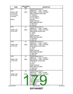
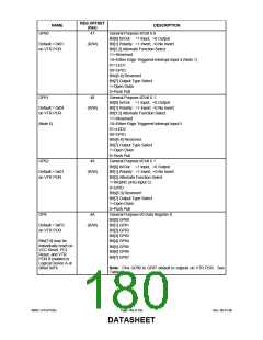
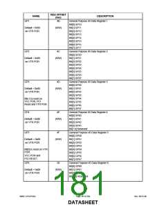
REG OFFSET
(hex)
NAME
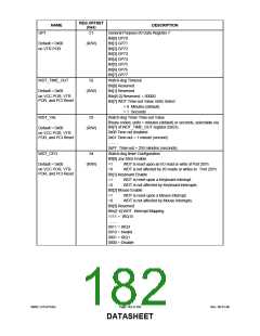
WDT_CTRL
DESCRIPTION
55
Watch-dog timer Control
Bit[0] Watch-dog Status Bit, R/W
Default = 0x00
(R/W)
=1
=0
WD timeout occurred
WD timer counting
on VCC POR and
VTR POR
Bit[2] is
Bit[1] Reserved
Write-Only
Bit[2] Force Timeout, W
Default = 0000000xb
on PCI Reset
=1
Forces WD timeout event; this bit is self-clearing
Bit[3] P20 Force Timeout Enable, R/W
Note: Bit[0] is not
cleared by PCI Reset
= 1
Allows rising edge of P20, from the Keyboard Controller,
to force the WD timeout event. A WD timeout event may still be
forced by setting the Force Timeout Bit, bit 2.
= 0
P20 activity does not generate the WD timeout event.
Note: The P20 signal will remain high for a minimum of 1us and
can remain high indefinitely. Therefore, when P20 forced timeouts
are enabled, a self-clearing edge-detect circuit is used to generate
a signal which is ORed with the signal generated by the Force
Timeout Bit.
Bit[7:4] Reserved. Set to 0
FAN Register
FAN
56
Bit[0] Fan Control
1=FAN pin is high
Default = 0x00
on VTR POR
(R/W)
0=bits[6:1] control the duty cycle of the
FAN pin.
Bit[6:1] Duty Cycle Control
Control the duty cycle of the FAN pin
000000 = pin is low
100000 = 50% duty cycle
111111 = pin is high for 63, low for 1
Bit[7] Fan Clock Select
This bit is used with the Fan Clock Source Select and the Fan
Clock Multiplier bits in the Fan Control register (0x58) to determine
the fan speed FOUT. See Different Modes for Fan in Table 61 on
page 124 in “Fan Speed Control and Monitoring” section.
The fan speed may be doubled through bit 2 of Fan Control
Register at 0x58.
Fan Control
58
Fan Control Register
Bit[0] Fan Clock Source Select
Default = 0x10
on VTR POR
(R/W)
This bit and the Fan Clock Multiplier bit is used with The Fan Clock
Select bit in the Fan register (0x56) to determine the fan speed
F
OUT. See Different Modes for Fan in Table 61 on page 124 in “Fan
Speed Control and Monitoring” section.
Bit[1] Reserved
Bit[2] Fan Clock Multiplier
0=No multiplier used
1=Double the fan speed selected by bit 0 of this register
and bit 7 of the Fan register
Bit[3] Reserved
Bit[5:4] FAN Count Divisor.
Clock scalar for adjusting the tachometer count. Default = 2.
00: divisor = 1
01: divisor = 2
10: divisor = 4
11: divisor = 8
Bit[7:6] Reserved
SMSC LPC47S45x
Page 183 of 259
Rev. 06-01-06
DATASHEET

 SMSC [ SMSC CORPORATION ]