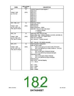
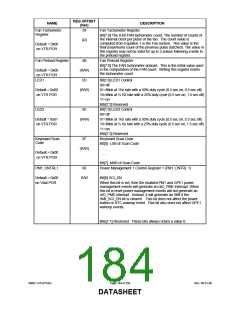
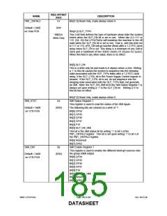
REG OFFSET
(hex)
NAME
DESCRIPTION
General Purpose I/0 Data Register 7
GP7
51
Bit[0] GP70
Default = 0x00
on VTR POR
(R/W)
Bit[1] GP71
Bit[2] GP72
Bit[3] GP73
Bit[4] GP74
Bit[5] GP75
Bit[6] GP76
Bit[7] GP77
WDT_TIME_OUT
Default = 0x00
52
Watch-dog Timeout
Bit[0] Reserved
(R/W)
Bit[1] Reserved
on VCC POR, VTR
POR, and PCI Reset
Bits[6:2] Reserved, = 00000
Bit[7] WDT Time-out Value Units Select
= 0 Minutes (default)
= 1 Seconds
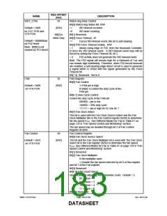
WDT_VAL
53
Watch-dog Timer Time-out Value
Binary coded, units = minutes (default) or seconds, selectable via
Bit[7] of WDT_TIME_OUT register (0x52).
Default = 0x00
(R/W)
0x00 Time out disabled
0x01 Time-out = 1 minute (second)
.........
on VCC POR, VTR
POR, and PCI Reset
0xFF Time-out = 255 minutes (seconds)
Watch-dog timer Configuration
Bit[0] Joy-Stick Enable
WDT_CFG
54
Default = 0x00
(R/W)
=1
=0
WDT is reset upon an I/O read or write of Port 201h
on VCC POR, VTR
POR, and PCI Reset
WDT is not affected by I/O reads or writes to Port 201h.
Bit[1] Keyboard Enable
=1
=0
WDT is reset upon a Keyboard interrupt.
WDT is not affected by Keyboard interrupts.
Bit[2] Mouse Enable
=1
=0
WDT is reset upon a Mouse interrupt.
WDT is not affected by Mouse interrupts.
Bit[3] Reserved
Bits[7:4] WDT Interrupt Mapping
1111 = IRQ15
.........
0011 = IRQ3
0010 = Invalid
0001 = IRQ1
0000 = Disable
SMSC LPC47S45x
Page 182 of 259
Rev. 06-01-06
DATASHEET

 SMSC [ SMSC CORPORATION ]