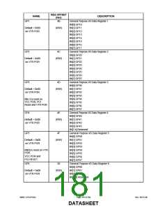
REG OFFSET
(hex)
NAME
DESCRIPTION
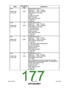
General Purpose I/0 bit 3.7
GP37
3A
Bit[0] In/Out : =1 Input, =0 Output
Bit[1] Polarity : =1 Invert, =0 No Invert
Bit[2] Alternate Function Select
1=A20M
Default = 0x01
on VTR POR
(R/W)
0=Basic GPIO function
Bits[6:3] Reserved
Bit[7] Output Type Select
1=Open Drain
0=Push Pull
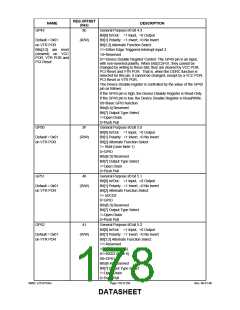
GP40
3B
General Purpose I/0 bit 4.0
Bit[0] In/Out : =1 Input, =0 Output
Bit[1] Polarity : =1 Invert, =0 No Invert
Bit[2] Alternate Function Select
1=DRVDEN0 (Note 3)
Default =0x01
on VTR POR
(R/W)
0=Basic GPIO function
Bits[6:3] Reserved
Bit[7] Output Type Select
1=Open Drain
0=Push Pull
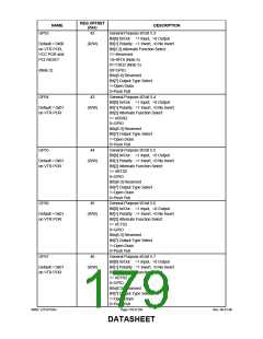
GP41
3C
General Purpose I/0 bit 4.1
Bit[0] In/Out : =1 Input, =0 Output
Bit[1] Polarity : =1 Invert, =0 No Invert
Bit[3:2] Alternate Function Select
11=Reserved
Default =0x01
on VTR POR
(R/W)
10=Either Edge Triggered Interrupt Input 2
01=DRVDEN1 (Note 3)
00=Basic GPIO function
Bits[6:4] Reserved
Bit[7] Output Type Select
1=Open Drain
0=Push Pull
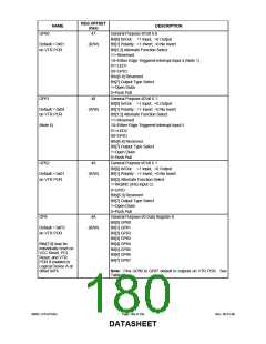
GP42
3D
General Purpose I/0 bit 4.2
Bit[0] In/Out : =1 Input, =0 Output
Bit[1] Polarity : =1 Invert, =0 No Invert
Bit[2] Alternate Function Select
1=IO_PME#
Default =0x01
on VTR POR
(R/W)
Note: Configuring this pin function as output with non-inverted
polarity will give an active low output signal. The output type can
be either open drain or push-pull.
0=Basic GPIO function
Bits[6:3] Reserved
Bit[7] Output Type Select
1=Open Drain
0=Push Pull
SMSC LPC47S45x
Page 177 of 259
Rev. 06-01-06
DATASHEET

 SMSC [ SMSC CORPORATION ]