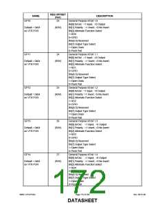
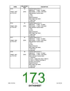
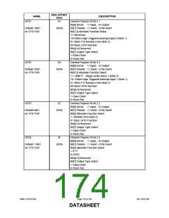
REG OFFSET
(hex)
NAME
DESCRIPTION
General Purpose I/0 bit 3.2
GP32
35
Bit[0] In/Out : =1 Input, =0 Output
Bit[1] Polarity : =1 Invert, =0 No Invert
Bit[2] Alternate Function Select
1= FAN_TACH
Default = 0x01
on VTR POR
(R/W)
0= GPIO
Bits[6:3] Reserved
Bit[7] Output Type Select
1=Open Drain
0=Push Pull
GP33
36
General Purpose I/0 bit 3.3
Bit[0] In/Out : =1 Input, =0 Output
Bit[1] Polarity : =1 Invert, =0 No Invert
Bit[2] Alternate Function Select
1=FAN
Default = 0x01
on VTR POR
Default = 0x00
on VCC POR
and PCI Reset
(R/W)
0= GPIO
Bits[6:3] Reserved
Bit[7] Output Type Select
1=Open Drain
0=Push Pull
(Note 2)
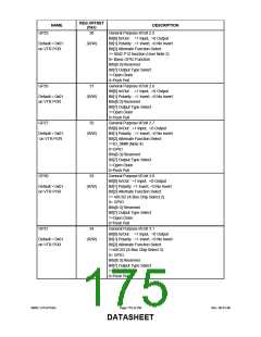
GP34
37
General Purpose I/0 bit 3.4
Bit[0] In/Out : =1 Input, =0 Output
Bit[1] Polarity : =1 Invert, =0 No Invert
Bit[2] Alternate Function Select
1=IRQINA (IRQ Input A)
0=GPIO
Default = 0x01
on VTR POR
(R/W)
Bits[6:3] Reserved
Bit[7] Output Type Select
1=Open Drain
0=Push Pull
GP35
38
General Purpose I/0 bit 3.5
Bit[0] In/Out : =1 Input, =0 Output
Bit[1] Polarity : =1 Invert, =0 No Invert
Bit[2] Alternate Function Select
1=IRQINB (IRQ Input B)
0=GPIO
Default = 0x01
on VTR POR
(R/W)
Bits[6:3] Reserved
Bit[7] Output Type Select
1=Open Drain
0=Push Pull
GP36
39
General Purpose I/0 bit 3.6
Bit[0] In/Out : =1 Input, =0 Output
Bit[1] Polarity : =1 Invert, =0 No Invert
Bit[2] Alternate Function Select
1= nKBDRST
Default = 0x01
on VTR POR
(R/W)
0=Basic GPIO function
Bits[6:3] Reserved
Bit[7] Output Type Select
1=Open Drain
0=Push Pull
SMSC LPC47S45x
Page 176 of 259
Rev. 06-01-06
DATASHEET

 SMSC [ SMSC CORPORATION ]