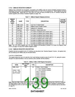
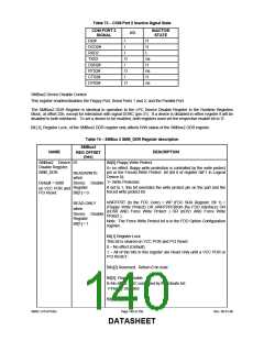
6.19 X-Bus Interface
The X-Bus interface is capable of performing I/O cycles initiated by either the SMBus or the LPC interface. This
interface allows the LPC47S45x to interface to as many as 4 external components that have an 8 bit data bus and
occupy up to 4 contiguous I/O address ports.
The LPC47S45x decodes I/O cycles received from the LPC interface and if the transaction is valid the X-Bus will
activate the appropriate chip select.
Note: Before initiating an I/O cycle, the SMBus or the LPC interface should verify that it has been granted access to
the X-Bus.
Note: External pullups are required on the nXRD and nXWR pins.
Note: The X-Bus interface is powered by VCC only.
6.19.1 I/O CYCLES
I/O cycles may be initiated on the X-Bus by either the SMBus or LPC interfaces. Since both interfaces can request
the X-Bus, a simple arbitration scheme has been implemented on a “first-come, first-serve” basis, where the request
not chosen is simply ignored. All I/O transactions will be decoded, but only the bus that wins arbitration will be given
access to the X-Bus interface. See section 6.18.3 X-Bus SMBus2/LPC Arbitration on page 137 for a more detailed
description of arbitrating access to the X-Bus.
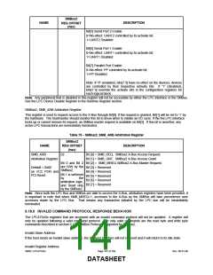
The X-bus chip selects XCS1, nXCS2, and nXCS3 have an associated disable bit. This bit allows each chip select to
be individually enabled or disabled. This bit is part of the X-bus Low Address Byte Configuration register.
The X-bus chip selects, XCS1, nXCS2, and nXCS3, base address register has an associated “write protect” bit that
can only be set once, and is reset by VCC POR and PCI Reset. When this bit is set, it prevents the base address
configuration registers (high byte and low byte) for each chip select from being written. This security feature ensures
that the base address and disable bit for each chip select can only be set by BIOS and cannot be corrupted by any
virus software. This bit is part of the X-bus Low Address Byte Configuration register.
Note: nXCS0 does not have the disable bit or the write protect bit so that it may be used to support snooping on port
80h.
Note: All the chip selects are active low except XCS1. This chip select was designed to support an LCD controller,
which needs an active high signal. See section 6.19.2 Supported LCD Controllers.
The read and write strobes have address setup and hold times, and pulse widths, that are compatible with X-Bus
timing of the Intel PIIX4. See the timing diagrams in the “Timing” section. The strobes will only become active during
an LPC cycle in which the LPC address matches the corresponding X-bus address or during an SMBus initiated cycle
in which the SMBus Command Code matches the corresponding chip select command code. When the read/write
strobes become active, the bus that wins arbitration will either read/write the data presented on the XD[7:0] pins.
SMBus Initiated I/O Cycles
The X-Bus interface may be accessed by the SMBus2 controller for I/O transactions. (See section 6.18 SMBus2
Slave Device) The X-Bus interface will decode the four MSB (i.e., bits[7:4]) of the command code received on the
SMBus. If the command code received matches one of the command codes defined in Table 69 then the appropriate
chip select will be made active. The four LSB (i.e., [3:0]) of the command code will be forwarded to address bits XA3
to XA0 respectively.
LPC Initiated I/O Cycles
The X-Bus interface may be accessed by the LPC interface for I/O transactions only. See section 6.3 LPC Interface
on page 24 for supported LPC I/O cycles. The chip select outputs are generated by circuitry in the LPC47S45x that
compares the LPC I/O address bits with the X-bus base I/O address configuration registers.
SMSC LPC47S45x
Page 143 of 259
Rev. 06-01-06
DATASHEET

 SMSC [ SMSC CORPORATION ]