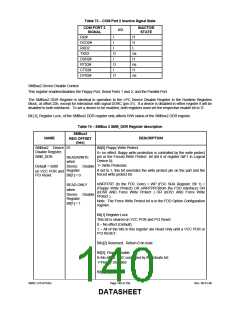
Table 73 − COM Port 2 Inactive Signal State
COM PORT 2
SIGNAL
INACTIVE
STATE
I/O
RI2#
I
H
DCD2#
RXD2
I
H
I
L
TXD2
O
I
na
H
DSR2#
RTS2#
CTS2#
DTR2#
O
I
na
H
O
na
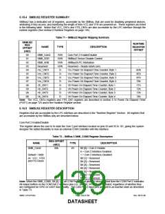
SMBus2 Device Disable Control
This register enables/disables the Floppy Port, Serial Ports 1 and 2, and the Parallel Port.
The SMBus2 DDR Register is identical in operation to the LPC Device Disable Register in the Runtime Registers
Block, at offset 22h, except for interaction with signal DDRC (pin 31). If a device is disabled in either register it will be
disabled to both interfaces. To set a device to be enabled, both registers must set the respective enable bit to ‘0’.
Bit [1], Register Lock, of the SMBus2 DDR register only affects R/W status of the SMBus2 DDR register.
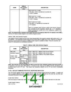
Table 74 − SMBus 2 SMB_DDR Register description
SMBus2
NAME
DESCRIPTION
Bit[0] Floppy Write Protect.
REG OFFSET
(hex)
SMBus2 Device 01
Disable Register,
SMB_DDR
0= no effect: floppy write protection is controlled by the write protect
pin or the Forced Write Protect bit (bit 0 of register 0xF1 in Logical
Device 0);
READ/WRITE
when
1= Write Protected.
Default = 0x00
Device Disable
Register
Bit[1] = 0
If set to 1, this bit overrides the write protect pin on the part and the
forced write protect bit.
on VCC POR and
PCI Reset.
nWRTPRT (to the FDC Core) = WP (FDC SRA Register, Bit 1) =
(Floppy Write Protect) OR nWRTPRT(from the FDD Interface) OR
(nDS0 AND Force Write Protect ) OR (nDS1 AND Force Write
Protect ).
READ-ONLY
when
Device Disable
Register
Bit[1] = 1
Note: The Force Write Protect bit is in the FDD Option Configuration
register.
Bit[1] Register Lock
This bit is cleared on VCC POR and PCI Reset.
0 – No effect (Default)
1 – All of the bits in this register are Read Only until a VCC POR or
PCI RESET.
Bits[2] Reserved. Return 0 on read.
Bit[3]: Floppy Enable.
0=No effect: FDC controlled by its activate bit;
1=Floppy Disabled
Bit[4] Reserved
SMSC LPC47S45x
Page 140 of 259
Rev. 06-01-06
DATASHEET

 SMSC [ SMSC CORPORATION ]