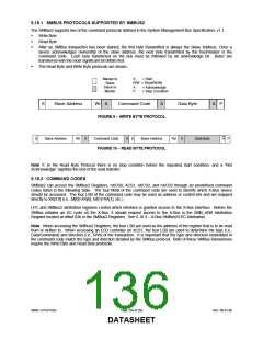
Bit 7 SMB_RST
The SMBus Reset bit D7 is used to reinitialize all the logic and registers in the SMBus block.
SMB_RST is active high and is not self-clearing. To properly reset the the SMBus block, write the SMB_RST bit to ‘1’
and then re-write the SMB_RST bit to ‘0’; i.e., the SMB_RST bit must be ‘0’ for normal device operation.
The SMB_RST bit is ‘0’ by default.
Bit 6 – Bit 3
RESERVED
Bit 2 CLK_DIV
The CLK_DIV bit D2 is used to divide the SMBus input clock by two.
When CLK_DIV = ‘0’ (default) the SMBus input clock is not divided; when CLK_DIV = ‘1’, the SMBus input clock, as
well as the SMBus output clock SCLK, is divided by two.
Bit 1 CLK_SEL
The CLK_SEL bit D1 is used to enable the SMBus input clock.
When CLK_SEL = ‘1’, the SMBus inout clock is enabled and the SMBus block can operate normally; when CLK_SEL
= ‘0’ (default), the input clock is stopped and the SMBus will not run.
The SMBus output clock SCLK frequency is determined by the CLK_SEL and CLK_DIV bits (Table 68).
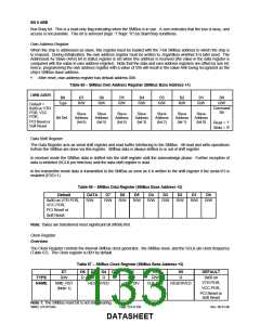
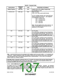
Table 68 − SMBus Clock Select Encoding
SMBUS CLOCK FREQUENCY
CONTROLS
DESCRIPTION
CLK_SEL
CLK_DIV
0
1
1
X
0
1
CLOCK OFF
SCLK = 100kHz
SCLK = 50kHz
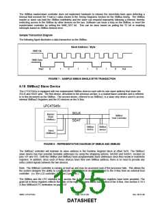
SMBus Timeouts
Overview
The SMBus is designed to provide a predictable communications link between a system and its devices. However
some devices, such as a Smart Battery using a microcontroller to support both bus and maintain battery data, may
require more time than might normally be expected. The following specifications take such devices into account
while maintaining a relatively predictable communications. The following are general comments on the SMBus’
timing:
The bus may be at 0 kHz when idle.
The FSMB Min is intended to dissuade components from taking too long to complete a transaction.
An idle bus can be detected by observing that both the clock and data remain high for longer than THIGH Max.
Every device must be able to recognize and react to a start condition at FSMB Max.
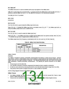
See the Timing Diagrams Section for the SMBUS timing.
SMBus Timeout
The SMBus controller will indicate a timeout error when any clock low (SCLK) exceeds the TTIMEOUT value
shown in SMBus timing table above.
Timeout errors are identified using the TE bit in the SMBus Status register (see Status Register section).
SMSC LPC47S45x
Page 134 of 259
Rev. 06-01-06
DATASHEET

 SMSC [ SMSC CORPORATION ]