The following is an example of how to program these bits for the Write Byte protocol.
To issue a start command:
−
−
−
−
load the data register with slave address
write to the control register to initiate a start condition (i.e., Bits[2:1] = 10) (see Note 1)
poll status register for a successful completed transaction (i.e., PIN bit = ‘0’ and LRB bit = ‘1’)
write NOP to the control register to prevent repeated start condition (i.e., Bits[2:1] = 00)
To issue a command/data byte:
−
−
load data register with command/data byte (see Note 1)
poll status register for a successful completed transaction (i.e., PIN bit = ‘0’ and LRB bit = ‘1’)
To issue a stop command:
−
−
write to the control register to initiate a stop condition (i.e., Bits[2:1] = 01) (see Note 1)
load the data register with dummy data (Note: This issues stop condition. )
(Note 1: ESO bit must be ‘1’ to shift serial data onto SMBus)
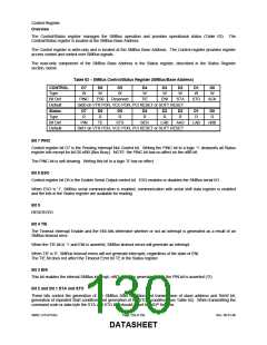
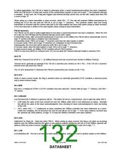
Table 64 − Instruction Table for Serial Bus Control
PRESENT MODE FUNCTION OPERATION
START
STA
STO
1
0
SLV/REC
Transmit START+address, remain
MST/TRM if R/nW=0; go to MST/REC if R/nW=1.
1
0
0
1
MST/TRM
REPEAT START Same as for SLV/REC
MST/REC;
MST/TRM
STOP READ;
STOP WRITE
Transmit STOP go to SLV/REC mode; Note 1
1
0
1
0
MST
DATA
CHAINING
Send STOP, START and address after last master
frame without STOP sent; Note 2
ANY
NOP
No operation; Note 3
Note 1: In master receiver mode, the last byte must be terminated with ACK bit high (‘negative acknowledge’).
Note 2: If both STA and STO are set high simultaneously in master mode, a STOP condition followed by a START
condition + address will be generated. This allows ‘chaining’ of transmissions without relinquishing bus control.
Note 3: All other STA and STO mode combinations not mentioned in Table 64 are NOPs.
Bit 0 ACK
This bit must be set normally to logic “1”. This causes the SMBus to send an acknowledge automatically after each
byte (this occurs during the 9th clock pulse). The bit is reset (to logic “0”) when the SMBus controller is operating in
master/receiver mode and requires no further data to be sent from the slave transmitter. This causes a negative
acknowledge on the SMBus, which halts further transmission from the slave device.
Status Register
Overview
The Status register, the read-only component of the SMBus Base Address, enables access to SMBus operational
status information.
Bit 7 PIN
Pending Interrupt Not. This bit is a status flag which is used to synchronize serial communication and is set to logic
“0” whenever the chip requires servicing. The PIN bit is normally read in polled applications to determine when an
SMBus byte transmission/reception is completed.
When acting as transmitter, PIN is set to logic “1” (inactive) each time the data register is written. In receiver mode,
the PIN bit is automatically set to logic “1” each time the data register is read.
After transmission or reception of one byte on the SMBus (nine clock pulses, including acknowledge) the PIN bit will
be automatically reset to logic “0” (active) indicating a complete byte transmission/reception. When the PIN bit is
subsequently set to logic “1” (inactive) all status bits will be reset to “0” on a BER (bus error) condition.
SMSC LPC47S45x
Page 131 of 259
Rev. 06-01-06
DATASHEET

 SMSC [ SMSC CORPORATION ]