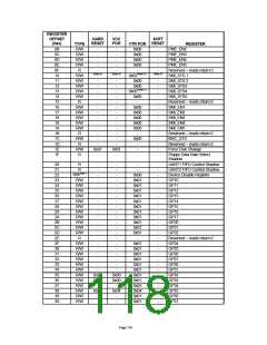
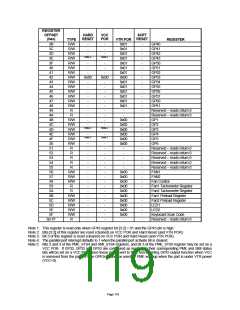
REGISTER
OFFSET
(hex)
HARD
RESET
VCC
POR
SOFT
RESET
TYPE
R/W
R/W
R/W
R/W
R/W
R/W
R/W
R/W
R/W
R/W
R/W
R/W
R/W
R/W
R
VTR POR
0x01
0x01
0x01
0x01
0x01
0x01
0x01
0x00
0x01
0x01
0x01
0x01
0x01
0x01
-
REGISTER
3B
3C
3D
3E
3F
40
41
42
43
44
45
46
47
48
49
4A
4B
4C
4D
4E
4F
50
51
-
-
-
-
-
-
-
-
-
-
-
-
-
-
-
-
-
-
-
-
-
-
-
-
-
-
-
-
-
-
-
-
-
-
-
-
-
-
-
-
-
-
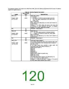
GP40
GP41
GP42
GP43
GP50
GP51
GP52
GP53
GP54
GP55
GP56
GP57
GP60
GP61
-
-
Note 2
Note 2
-
-
-
-
-
-
0x00
0x00
-
-
-
-
-
-
-
-
-
-
-
-
-
-
-
-
-
-
Reserved – reads return 0
Reserved – reads return 0
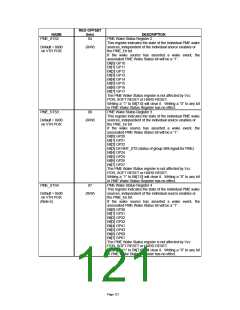
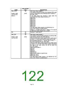
GP1
R
-
R/W
R/W
R/W
R/W
R/W
R/W
R
R
R
R
R
0x00
0x00
0x00
0x00
0x00
0x00
-
-
-
-
-
0x00
0x00
0x50
0x00
0x00
0x00
0x00
0x00
0x00
0x00
-
-
-
GP2
GP3
GP4
GP5
Note 2
Note 2
-
-
Note 3
Note 3
-
-
-
-
-
-
-
-
-
-
-
-
-
-
-
-
-
-
-
-
-
-
-
-
-
-
-
-
-
-
-
-
-
-
GP6
Reserved – reads return 0
Reserved – reads return 0
Reserved – reads return 0
Reserved – reads return 0
Reserved – reads return 0
FAN1
52
53
54
55
56
57
58
59
5A
5B
5C
5D
5E
5F
60-7F
R/W
R/W
R/W
R
FAN2
Fan Control
Fan1 Tachometer Register
Fan2 Tachometer Register
Fan1 Preload Register
Fan2 Preload Register
LED1
R
R/W
R/W
R/W
R/W
R/W
R
LED2
Keyboard Scan Code
Reserved – reads return 0
Note 1: This register is read-only when GP43 register bit [3:2] = 01 and the GP43 pin is high.
Note 2: Bits [3:2] of this register are reset (cleared) on VCC POR and Hard Reset (and VTR POR).
Note 3: Bit 3 of this register is reset (cleared) on VCC POR and Hard Reset (and VTR POR).
Note 4: The parallel port interrupt defaults to 1 when the parallel port activate bit is cleared.
Note 5: Bits 2 and 3 of the PME_STS4 and SMI_STS4 registers, and bit 3 of the PME_STS5 register may be set on a
VCC POR. If GP32, GP33 and GP53 are configured as input, then their corresponding PME and SMI status
bits will be set on a VCC POR since these pins revert to their non-inverting GPIO output function when VCC
is removed from the part. These GPIOs cannot be used for PME wakeup when the part is under VTR power
(VCC=0).
Page 119

 SMSC [ SMSC CORPORATION ]