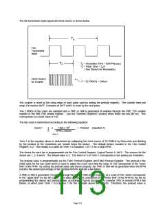
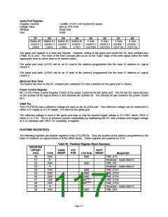
Game Port Register
Register Location:
Default Value:
Attribute:
<GAME_PORT>+0h System I/O Space
00h on VTR POR
Read-Only
8-bits
Size:
D7
D6
D5
D4
D3
D2
D1
D0
Button #2 Button #1 Button #2 Button #1
Y-Axis
X-Axis
Y-Axis
X-Axis
Joystick 2 Joystick 2 Joystick 1 Joystick 1 Joystick 2 Joystick 2 Joystick 1 Joystick 1
(J2B2) (J2B1) (J1B2) (J1B1) (OUT2B) (OUT2A) (OUT1B) (OUT1A)
The game port register is a read-only register. However, writing to the game port resets the RC time constant pins
(TIMA, B) to zero. The reset of the time constant pins occur on the “back” edge of the write signal (when the write
signal goes from its active state to its inactive state).
The game port read (JOYR) will be an IO read to the address programmed into the base IO address in Logical
Device 9.
The game port write (JOYW) will be an IO write to the address programmed into the base IO address in Logical
Device 9.
Minimum Rise Time
The fastest rise time on the RC constant pins (minimum RC time constant) for the game port is 20usec.
Power Control Register
Bit 2 in the Power Control Register (CR22) is the power control bit for the game port. This bit has the same function
as the activate bit for logical device 9 and shadows the activate bit. The activate bit also shadows the power control
bit 2.
VREF Pin
The LPC47M10x has a reference voltage pin input on pin 44 of the part. This reference voltage can be connected to
either a 5V supply or a 3.3V supply. It is used for the game port.
The reference voltage is used in the game port logic so that the joystick trigger voltage is 2/3 VREF where VREF is
either 5V or 3.3V. This is to preserve joystick compatibility by maintaining the RC time constant reset trigger voltage
of 3.3V (nominal) with VREF=5V (nominal), if required.
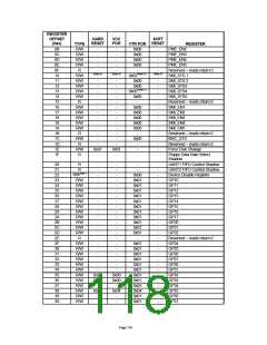
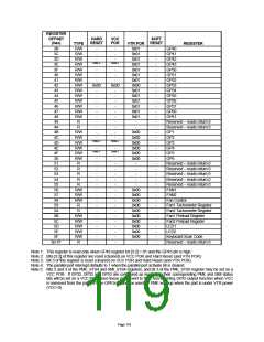
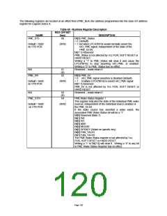
RUNTIME REGISTERS
The following registers are runtime registers in the LPC47M10x. They are located at the address programmed in the
Base I/O Address in Logical Device A at the offset shown. These registers are powered by VTR.
Table 59 - Runtime Register Block Summary
REGISTER
OFFSET
(hex)
HARD
RESET
VCC
POR
SOFT
RESET
TYPE
R/W
R
R/W
R
R/W
R/W
R/W
R/W
R/W
R
VTR POR
0x00
-
REGISTER
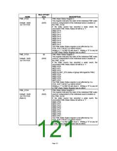
PME_STS
Reserved – reads return 0
PME_EN
Reserved – reads return 0
PME_STS1
PME_STS2
PME_STS3
PME_STS4
PME_STS5
Reserved – reads return 0
PME_EN1
00
01
02
03
04
05
06
07
08
09
0A
-
-
-
-
-
-
-
-
-
-
-
-
-
-
-
-
-
-
-
-
-
-
-
-
-
-
-
-
-
-
-
-
-
0x00
-
0x00
0x00
0x00
0x00(Note 5)
0x00(Note 5)
-
R/W
0x00
Page 117

 SMSC [ SMSC CORPORATION ]