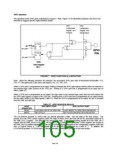
GPIO Operation
The operation of the GPIO ports is illustrated in Figure 4. Note: Figure 7 is for illustration purposes only and is not
intended to suggest specific implementation details.
GPIO
GPIO
Configuration
Register bit-1
(Polarity)
Configuration
Register bit-0
(Input/Output)
D-TYPE
SD-bit
D
Q
GPx_nIOW
GPx_nIOR
GPIO
PIN
0
1
Transparent
Q
D
GPIO
Data Register
Bit-n
FIGURE 7 - GPIO FUNCTION ILLUSTRATION
Note: When the following functions are selected, the associated GPIO pins have bi-directional functionality: P12,
P16, P17 and game port x-axis and y-axis inputs (J1X, J1Y, J2X, J2Y).
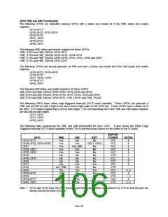
When a GPIO port is programmed as an input, reading it through the GPIO data register latches either the inverted or
non-inverted logic value present at the GPIO pin. Writing to a GPIO port that is programmed as an input has no
effect (Table 57).
When a GPIO port is programmed as an output, the logic value or the inverted logic value that has been written into
the GPIO data register is output to the GPIO pin. Reading from a GPIO port that is programmed as an output returns
the last value written to the data register (Table 57). When the GPIO is programmed as an output, the pin is excluded
from the PME and SMI logic.
TABLE 57 - GPIO Read/Write Behavior
HOST
OPERATION
READ
GPIO INPUT PORT
GPIO OUTPUT PORT
LATCHED VALUE OF GPIO PIN
NO EFFECT
LAST WRITE TO GPIO DATA REGISTER
BIT PLACED IN GPIO DATA REGISTER
WRITE
The LPC47M10x provides 31 GPIOs that can directly generate a PME. See the table in the next section. The
polarity bit in the GPIO control registers select the edge on these GPIO pins that will set the associated status bit in
the PME_STS 2 register. The default is the low-to-high edge. If the corresponding enable bit in the PME_EN 2
register and the PME_EN bit in the PME_EN register is set, a PME will be generated. These registers are located in
the PME_BLK of runtime registers which are located at the address contained in the configuration registers 0x60 and
0x61 in Logical Device A. The PME status bits for the GPIOs are cleared on a write of ‘1’. In addition, the
LPC47M10x provides 19 GPIOs that can directly generate an SMI. See the table in the next section.
Page 105

 SMSC [ SMSC CORPORATION ]