Three Port 10/100 Managed Ethernet Switch with MII
Datasheet
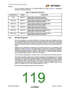
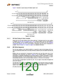
Figure 8.1 illustrates a typical single and multiple register read.
nSCS
1
0
1
1
1
2
1
3
1
4
1
5
1
6
1
7
1
8
1
9
4
5
4
6
4
7
4
8
X
X
1
2
3
4
5
6
7
8
9
X
X
...
SCK (active low)
SCK (active high)
1
0
1
1
1
2
1
3
1
4
1
5
1
6
1
7
1
8
1
4
5
4
6
4
7
4
8
...
1
2
3
4
5
6
7
8
9
9
Instruction
Address
...
X
0
0
0
0
0
0
1
1
A9 A8 A7 A6 A5 A4 A3 A2
X
X
SI
Data
D
31
D
30
D
29
...
Z
D2 D1 D0
X
Z
SO
Single Register Read
nSCS
1
0
1
1
1
2
1
3
1
4
1
5
1
6
1
7
1
8
1
9
X
X
1
2
3
4
5
6
7
8
9
...
...
...
X
X
SCK (active low)
1
0
1
1
1
2
1
3
1
4
1
5
1
6
1
7
1
8
1
1
2
3
4
5
6
7
8
9
...
SCK (active high)
9
Instruction
Address
...
...
X
0
0
0
0
dec inc
1
1
A9 A8 A7 A6 A5 A4 A3 A2
X
X
X
SI
Data 1... ...…Data m
...…Data n
Data m+1...
D
31
D
30
D
29
D
D
D
Z
D2 D1 D0
D2 D1 D0
X
Z
SO
31
30
29
Multiple Register Reads
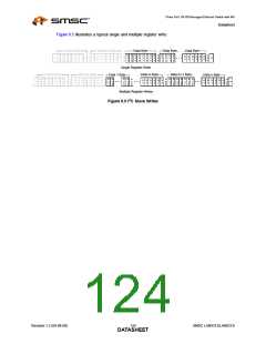
Figure 8.1 SPI Reads
8.4.1.1
SPI Read Polling for Reset Complete
During reset, the SPI slave interface will not return valid data. To determine when the reset condition
is complete, the Byte Order Test Register (BYTE_TEST) should be polled. Once the correct pattern is
read, the interface can be considered functional. At this point, the READY bit in the Hardware
Configuration Register (HW_CFG) can be polled to determine when the device initialization is
complete. Refer to Section 4.2, "Resets," on page 41 for additional information.
8.4.2
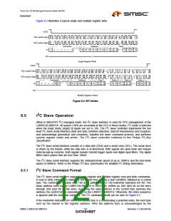
SPI Write Sequence
The SPI slave interface of the LAN9313/LAN9313i is selected for writes by first bringing nSCS low.
The SI pin should then driven with an 8-bit write instruction, followed by the 8-bit address and then the
data.
Multiple writes are performed by continuing the clock pulses and input data while nSCS is low.
Depending on the instruction (as shown in Table 8.10), the internal address is incremented,
decremented, or maintained. Maintaining an fixed internal address is useful for “bit-banging”. For auto-
incrementing instructions, once the internal address reaches its maximum, it rolls over to 0. For auto-
decrementing instructions, once the internal address reaches 0, it rolls over to its maximum.
The nSCS input is brought high to conclude the cycle. The SO output is three-stated throughout the
entire write sequence.
The data write to the register occurs after the 32-bits are input. In the event that 32-bits are not written
when the nSCS is returned high, the write is considered invalid and the register is not affected. Multiple
registers may be written in a multiple write cycle, each one being written after 32-bits.
SPI writes must not be performed to unused register addresses.
Revision 1.2 (04-08-08)
120
SMSC LAN9313/LAN9313i
DATASHEET

 SMSC [ SMSC CORPORATION ]