Three Port 10/100 Managed Ethernet Switch with MII
Datasheet
8.3
SPI/I2C Slave Controller
2
The SPI/I C slave controller functionality is dependant on the management mode of the
2
2
LAN9313/LAN9313i. When in MAC/PHY I C managed modes, the I C controller is enabled. When in
2
MAC/PHY SPI managed modes, the SPI controller is enabled. The SPI/I C serial management pins
functionality and characteristics differ dependant on the selected modes as summarized in Table 8.9.
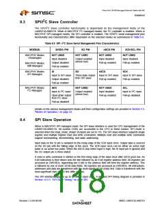
Table 8.9 SPI / I2C Slave Serial Management Pins Characteristics
MODE(S)
SI/SDA PIN
NOT USED
SO PIN
nSCS PIN
NOT USED
SCK/SCL PIN
MAC/PHY Modes
Unmanaged
NOT USED
NOT USED
Input disabled
Output disabled
Pull-up enabled
Output enabled
(driven low)
Input disabled
Input disabled
Pull-up enabled
Pull-up enabled
MAC/PHY Modes
SMI Managed
MAC/PHY Modes
SPI Managed
SI
SO
nSCS
SCK
Input to SPI slave
Output disabled
Pull-up enabled
Three-state output
from SPI slave
Input to SPI slave
Pull-up enabled
Input to SPI slave
Pull-up enabled
MAC/PHY Modes
I C Managed
SDA
NOT USED
NOT USED
SCL
2
2
2
Input to I C slave
Output enabled
(driven low)
Input disabled
Pull-up enabled
Input to I C slave
Open-drain output
from I C slave
Pull-up disabled
2
Pull-up disabled
Details on the various management modes and their configuration settings are provided in Section 2.3,
"Modes of Operation," on page 23.
8.4
SPI Slave Operation
When in MAC/PHY SPI managed mode, the SPI slave interface is used for CPU management of the
LAN9313/LAN9313i. All system CSRs are accessible to the CPU in these modes. SPI mode is
selected when the mngt_mode_strap[1:0] inputs are set to 11b. The SPI slave interface supports single
register and multiple register read and write commands. Multiple read and multiple write commands
support incrementing, decrementing, and static addressing.
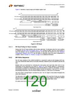
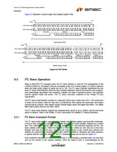
Input data on the SI pin is sampled on the rising edge of the SCK input clock. Output data is sourced
on the SO pin with the falling edge of the clock. The SCK input clock can be either an active high
pulse or an active low pulse. When the nSCS chip select input is high, the SI input pin is ignored and
the SO output pin is three-stated.
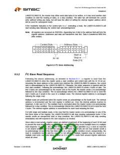
A read or write command is started on the first rising edge of the input clock after nSCS goes low. An
8-bit instruction is then driven onto the line followed by an 8-bit register address field. All registers are
accessed as DWORDs. Appending two 0 bits to the address field will form the register address. This
is followed by one or more 32-bit data fields. All registers are accessed as DWORDs. All instructions,
addresses and data are transferred with the most-significant bit (msb) first. Data is transferred with the
most-significant byte (MSB) first (little endian).
The SPI interface supports up to a 10MHz input clock. A detailed SPI timing diagram is provided in
Section 14.5.5, "SPI Slave Timing," on page 393.
Revision 1.2 (04-08-08)
118
SMSC LAN9313/LAN9313i
DATASHEET

 SMSC [ SMSC CORPORATION ]