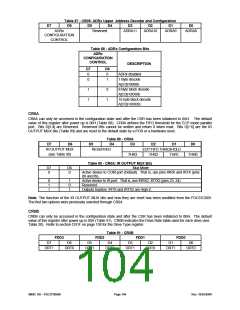
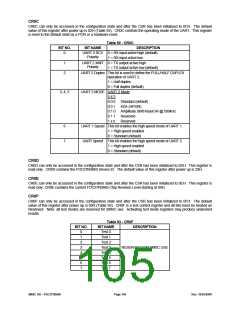
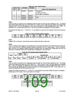
CR0C
CR0C can only be accessed in the configuration state and after the CSR has been initialized to 0CH. The default
value of this register after power up is 02H (Table 92). CR0C controls the operating mode of the UART. This register
is reset to the default state by a POR or a hardware reset.
Table 92 - CR0C
BIT NO.
BIT NAME
DESCRIPTION
0
UART 2 RCV 0 = RX input active high (default).
Polarity
1 = RX input active low.
1
2
UART 2 XMIT 0 = TX output active high.
Polarity
1 = TX output active low (default).
UART 2 Duplex This bit is used to define the FULL/HALF DUPLEX
operation of UART 2.
1 = Half duplex
0 = Full duplex (default)
UART 2 MODE UART 2 Mode
5 4 3
3, 4, 5
0 0 0 Standard (default)
0 0 1 IrDA (HPSIR)
0 1 0 Amplitude Shift Keyed IR @ 500kHz
0 1 1 Reserved
1 x x
Reserved
6
7
UART 1 Speed This bit enables the high speed mode of UART 1.
1 = High speed enabled
0 = Standard (default)
UART Speed This bit enables the high speed mode of UART 2.
1 = High speed enabled
0 = Standard (default)
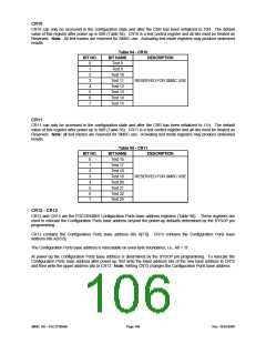
CR0D
CR0D can only be accessed in the configuration state and after the CSR has been initialized to 0DH. This register is
read only. CR0D contains the FDC37N3869 Device ID. The default value of this register after power up is 29H.
CR0E
CR0E can only be accessed in the configuration state and after the CSR has been initialized to 0EH. This register is
read only. CR0E contains the current FDC37N3869 Chip Revision Level starting at 00H.
CR0F
CR0F can only be accessed in the configuration state and after the CSR has been initialized to 0FH. The default
value of this register after power up is 00H (Table 93). CR0F is a test control register and all bits must be treated as
Reserved. Note: all test modes are reserved for SMSC use. Activating test mode registers may produce undesired
results.
Table 93 - CR0F
BIT NO.
BIT NAME
Test 0
Test 1
Test 2
Test 3
Test 4
Test 5
Test 6
Test 7
DESCRIPTION
0
1
2
3
4
5
6
7
RESERVED FOR SMSC USE
SMSC DS – FDC37N3869
Page 105
Rev. 10/25/2000

 SMSC [ SMSC CORPORATION ]